JCK3024D12

DCDC
Specification
30 Watts
2:1 Input Range
Operating Temperature 40 °C to +75 °C
Single and Dual Outputs
High Efficiency Up to 92%
Remote On/Off
1600 VDC Isolation
3 Year Warranty
JCK Series
Input
Input Voltage Range 12 V (9-18 VDC),
24 V (18-36 VDC),
48 V (36-75 VDC)
Input Current See table
Undervoltage Lockout 12 V models: ON 8.6 V, OFF 7.9 V typical
24 V models: ON 17.8 V, OFF 16 V typical
48 V models: ON 33.5 V, OFF 30.5 V typical
Input Reflected Ripple 20 mA pk-pk through 12 uH inductor
Current
Input Surge 12 V models 25 VDC for 100 ms
24 V models 50 VDC for 100 ms
48 V models 100 VDC for 100 ms
Input Filter Pi network
Output
Output Voltage See table
Output Voltage Trim ±10% on single outputs models only
Start Up Delay 30 ms max
Minimum Load No minimum load required
Line Regulation ±0.5% max
Load Regulation Single output models: ±0.5% max
Dual output models: ±1% max
balanced outputs
Cross Regulation ±5% (see note 2)
Setpoint Accuracy ±1%
Ripple & Noise 100 mV pk-pk,
20 MHz bandwidth (see note 3)
Transient Response 3% max deviation, recovery to within
1% in <250 µs for a 25% load change
Temperature 0.02%/˚C
Coefficient
Overvoltage Protection 3.3 V models: 3.9 V typical
5 V models: 6.2 V typical
12 V models: 15 V typical
15 V models: 18 V typical
±5 V models: ±6.2 V typical
±12 V models: ±15 V typical
±15 V models: ±18 V typical
Overload Protection >150% of full load
Short Circuit Protection Trip & restart (Hiccup mode),
auto recovery
Remote On/Off • See application notes
Maximum Capacitive See table
Load
xppower.com
General
Efficiency See table
Isolation 1600 VDC Input to Output
1600 VDC Input to Case
1600 VDC Output to Case
Isolation Capacitance 1500 pF typical
Switching Frequency 330 kHz typical
Power Density 37.5 W/in
3
MTBF 430 kHrs min to MIL-HDBK-217F
at 25 ˚C, GB
Environmental
Operating Temperature • -40 °C to 75 °C, see derating curve
Case Temperature +105 ˚C max
Cooling Convection-cooled
Operating Humidity 5-95% RH, non-condensing
Storage Temperature -40 ˚C to +125 ˚C
EMC
Emissions EN55022 level A conducted & radiated
with external components, see application
notes
ESD Immunity EN61000-4-2, level 3, Perf Criteria A
EFT/Burst EN61000-4-4, level 3, Perf Criteria A
(4)
Surge EN61000-4-5, installation class 3,
Perf Criteria A
(4)
Conducted Immunity EN61000-4-6, 10 Vrms, Perf Criteria A
Magnetic Field EN61000-4-8, 1 A/m, Perf Criteria A
13-Jan-14
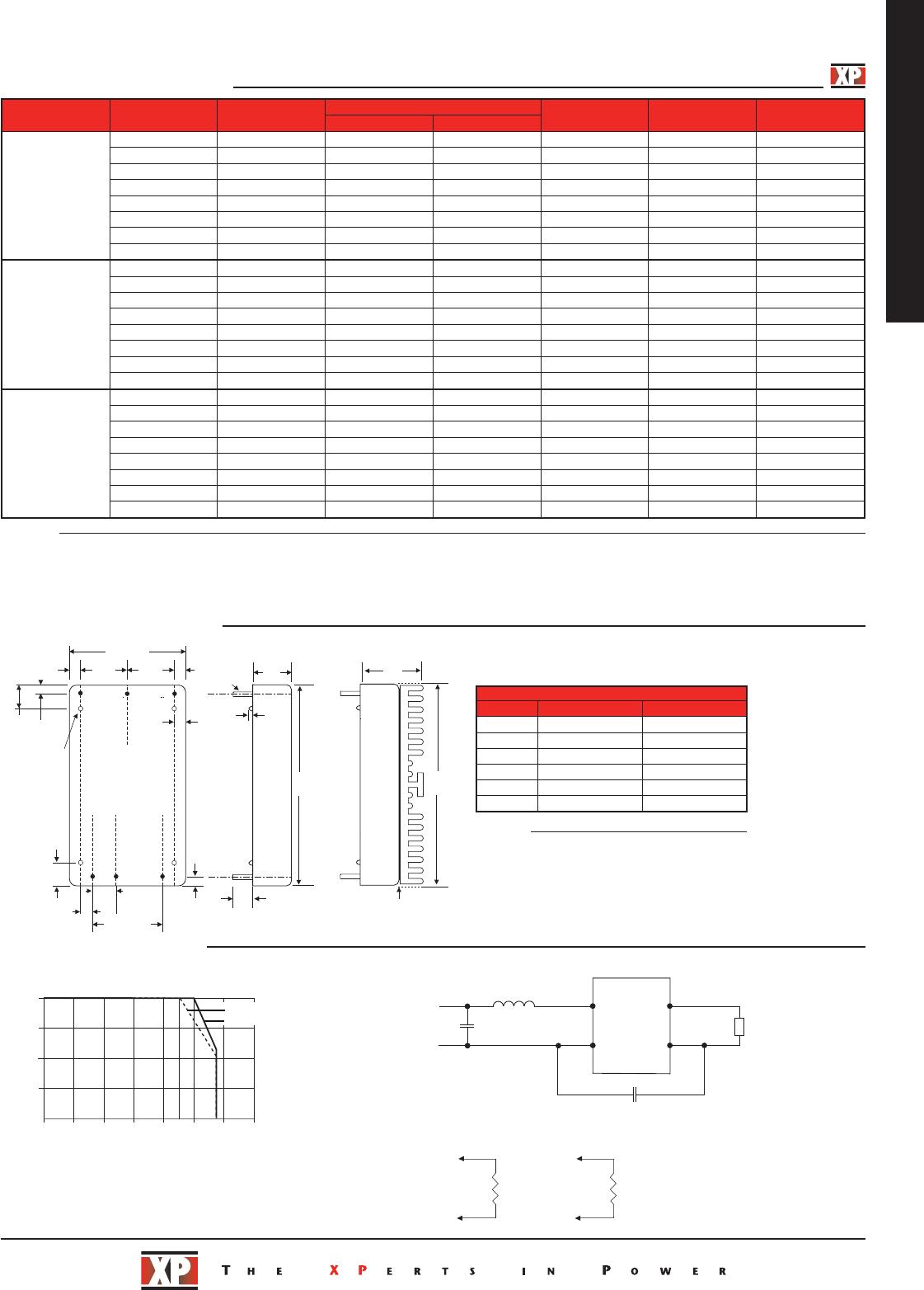
Input Voltage Output Voltage Output Current
Input Current
(1)
Maximum
Capacitive Load
Efficiency Model Number
No Load Full Load
9-18 VDC
3.3 V 8.00 A 80 mA 2426 mA 20000 µF 89% JCK3012S3V3
5.0 V 6.00 A 180 mA 2874 mA 14000 µF 91% JCK3012S05
5.1 V 6.00 A 160 mA 2874 mA 14000 µF 92% JCK3012S5V1
12.0 V 2.50 A 30 mA 2809 mA 2000 µF 91% JCK3012S12
15.0 V 2.00 A 30 mA 2809 mA 2000 µF 92% JCK3012S15
±5.0 V ±3.00 A 180 mA 2874 mA ±3000 µF 89% JCK3012D05
±12.0 V ±1.25 A 50 mA 2874 mA ±1250 µF 90% JCK3012D12
±15.0 V ±1.00 A 50 mA 2874 mA ±1000 µF 91% JCK3012D15
18-36 VDC
3.3 V 8.00 A 70 mA 1185 mA 20000 µF 91% JCK3024S3V3
5.0 V 6.00 A 100 mA 1420 mA 14000 µF 92% JCK3024S05
5.1 V 6.00 A 100 mA 1448 mA 14000 µF 92% JCK3024S5V1
12.0 V 2.50 A 20 mA 1436 mA 2000 µF 92% JCK3024S12
15.0 V 2.00 A 40 mA 1420 mA 2000 µF 92% JCK3024S15
±5.0 V ±3.00 A 100 mA 1437 mA ±3000 µF 90% JCK3024D05
±12.0 V ±1.25 A 40 mA 1453 mA ±1250 µF 91% JCK3024D12
±15.0 V ±1.00 A 50 mA 1437 mA ±1000 µF 91% JCK3024D15
36-75 VDC
3.3 V 8.00 A 50 mA 593 mA 20000 µF 90% JCK3048S3V3
5.0 V 6.00 A 70 mA 702 mA 14000 µF 91% JCK3048S05
5.1 V 6.00 A 70 mA 724 mA 14000 µF 91% JCK3048S5V1
12.0 V 2.50 A 30 mA 718 mA 2000 µF 91% JCK3048S12
15.0 V 2.00 A 30 mA 710 mA 2000 µF 91% JCK3048S15
±5.0 V ±3.00 A 70 mA 710 mA ±3000 µF 90% JCK3048D05
±12.0 V ±1.25 A 50 mA 718 mA ±1250 µF 90% JCK3048D12
±15.0 V ±1.00 A 40 mA 718 mA ±1000 µF 90% JCK3048D15
DCDC
JCK30
Notes
1. Input current specified at nominal input.
2. Cross regulation for duals is ±5% when one output is at 100% and the other is
varied between 25% and 100%.
3. Measured with 1 µF ceramic capacitor across output rails.
4. A 220 µF/250 V capacitor across the input is required in order to meet
EN61000-4-4 and EN61000-4-5.
5. For heatsink option add ‘-HK’ to the end of the part number.
0.10
(2.54)
0.20
(5.08)
0.10
(2.54)
0.60 (15.24)
0.20
(5.08)
0.10
(2.54)
0.40
(10.16)
0.40
(10.16)
1.0 (25.4)
0.10
(2.54)
0.10
(2.54)
4 5
1
2
3
6
Bottom View
0.10
(2.54)
0.20
(5.0)
DIA.
0.04
(1.00)
0.02
(0.50)
0.40
(10.16)
0.20
(5.08)
min
2.00
(50.80)
Ø 0.04
(1.00)
Thermal Pad
2.00
(50.80)
0.64
(16.3)
Optional heatsink (-HK)
Mechanical Details
Application Notes
-40 -20 0 20 40 60 80 100
50 75
25
50
75
100
Ambient Temperature (ºC)
Load (%)
0
with heat-sink
without heat-sink
Derating Curve
PIN CONNECTIONS
Pin Single Dual
1 +Vin +Vin
2 -Vin -Vin
3 Remote On/Off Remote On/Off
4 +Vout +Vout
5 -Vout Com
6 Trim -Vout
Remote On/Off Control
Output On >3.0 VDC or open circuit
Output Off <1.2 VDC or short circuit pins 2 & 3
1. All dimensions are in inches (mm).
2. Weight: 0.07 lbs (31 g) approx
3. Pin diameter: 0.04 ±0.002 (1.0 ±0.05)
4. Pin pitch tolerance: ±0.014 (±0.35)
5. Case tolerance: ±0.02 (±0.5)
Notes
12 µH
220 µF, 100 V
470 pF, 2 kV
+
-
+Vin
DC/DC
Converter
-Vout-Vin
LOAD
Input Filter
Models and Ratings
External Output Trim
R trim-up R trim-down
6
5
6
4
Output can be externally
trimmed using this method.
Contact sales for details.

JCK3024D12

Mfr. #:
Manufacturer:
Description:
DC DC CONVERTER +/-12V 30W
Lifecycle:
New from this manufacturer.
Delivery:
DHL FedEx Ups TNT EMS
Payment:
T/T Paypal Visa MoneyGram Western Union