LTC3410ESC6-1.5#TRPBF

7
LTC3410
3410fb
OPERATIO
U
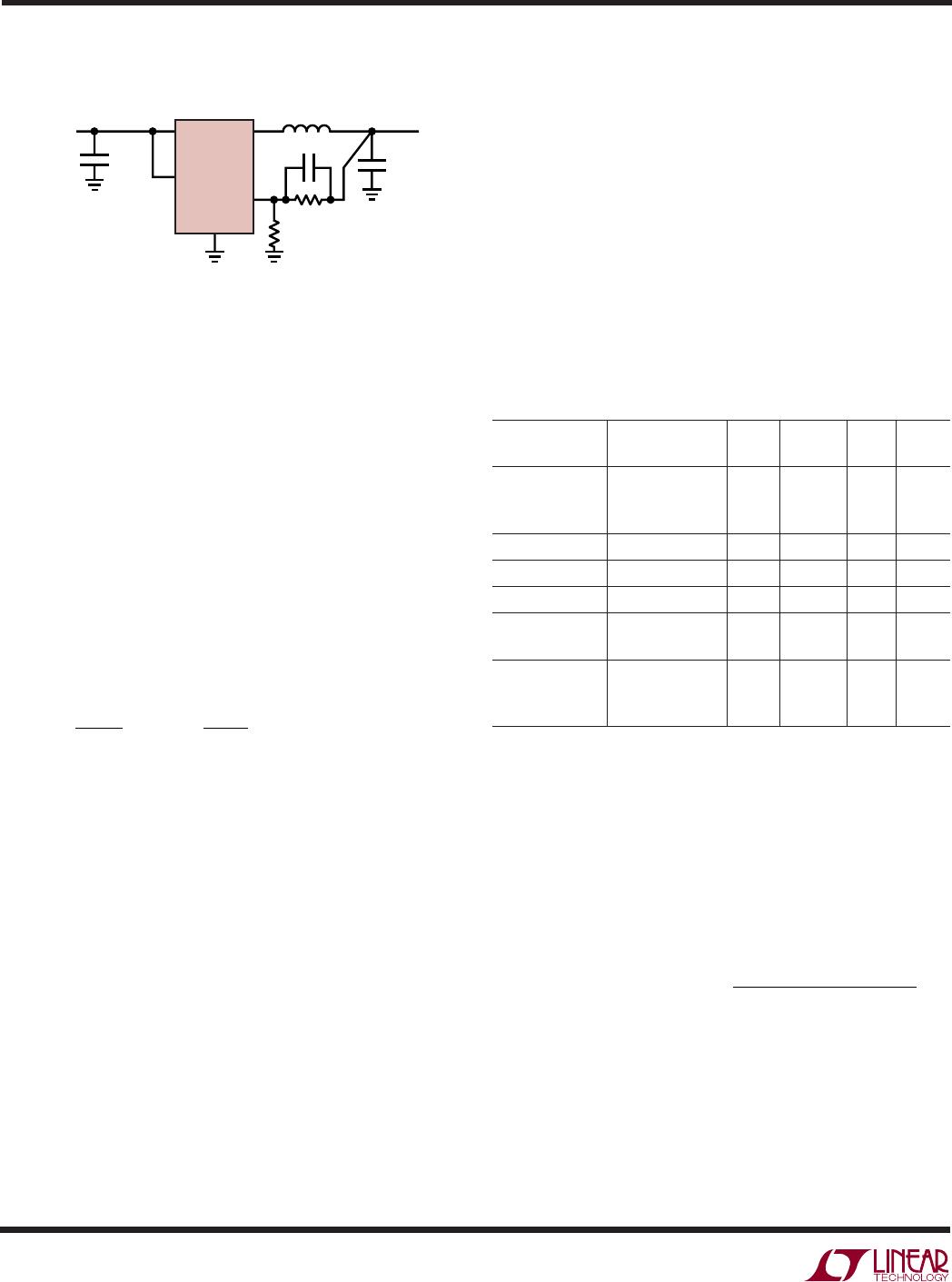
(Refer to Functional Diagram)
Main Control Loop
The LTC3410 uses a constant frequency, current mode
step-down architecture. Both the main (P-channel
MOSFET) and synchronous (N-channel MOSFET) switches
are internal. During normal operation, the internal top
power MOSFET is turned on each cycle when the oscillator
sets the RS latch, and turned off when the current com-
parator, I
COMP
, resets the RS latch. The peak inductor
current at which I
COMP
resets the RS latch, is controlled by
the output of error amplifier EA. The V
FB
pin, described in
the Pin Functions section, allows EA to receive an output
feedback voltage from an external resistive divider. When
the load current increases, it causes a slight decrease in
the feedback voltage relative to the 0.8V reference, which
in turn, causes the EA amplifier’s output voltage to in-
crease until the average inductor current matches the new
load current. While the top MOSFET is off, the bottom
MOSFET is turned on until either the inductor current
starts to reverse, as indicated by the current reversal
comparator I
RCMP
, or the beginning of the next clock cycle.
Burst Mode Operation
The LTC3410 is capable of Burst Mode operation in which
the internal power MOSFETs operate intermittently based
on load demand.
When the converter is in Burst Mode operation, the peak
current of the inductor is set to approximately 70mA re-
gardless of the output load. Each burst event can last from
a few cycles at light loads to almost continuously cycling
with short sleep intervals at moderate loads. In between
these burst events, the power MOSFETs and any unneeded
circuitry are turned off, reducing the quiescent current to
26µA. In this sleep state, the load current is being supplied
solely from the output capacitor. As the output voltage
droops, the EA amplifier’s output rises above the sleep
threshold signaling the BURST comparator to trip and turn
the top MOSFET on. This process repeats at a rate that is
dependent on the load demand.
Short-Circuit Protection
When the output is shorted to ground, the frequency of the
oscillator is reduced to about 310kHz, 1/7 the nominal
frequency. This frequency foldback ensures that the in-
ductor current has more time to decay, thereby preventing
runaway. The oscillator’s frequency will progressively
increase to 2.25MHz when V
FB
rises above 0V.
Dropout Operation
As the input supply voltage decreases to a value approach-
ing the output voltage, the duty cycle increases toward the
maximum on-time. Further reduction of the supply volt-
age forces the main switch to remain on for more than one
cycle until it reaches 100% duty cycle. The output voltage
will then be determined by the input voltage minus the
voltage drop across the P-channel MOSFET and the
inductor.
Another important detail to remember is that at low input
supply voltages, the R
DS(ON)
of the P-channel switch
increases (see Typical Performance Characteristics).
Therefore, the user should calculate the power dissipation
when the LTC3410 is used at 100% duty cycle with low
input voltage (See Thermal Considerations in the Applica-
tions Information section).
Slope Compensation and Inductor Peak Current
Slope compensation provides stability in constant fre-
quency architectures by preventing subharmonic oscilla-
tions at high duty cycles. It is accomplished internally by
adding a compensating ramp to the inductor current
signal at duty cycles in excess of 40%. Normally, this
results in a reduction of maximum inductor peak current
for duty cycles >40%. However, the LTC3410 uses a
patented scheme that counteracts this compensating
ramp, which allows the maximum inductor peak current
to remain unaffected throughout all duty cycles.
8
LTC3410
3410fb
The basic LTC3410 application circuit is shown in Figure 1.
External component selection is driven by the load require-
ment and begins with the selection of L followed by C
IN
and
C
OUT
.
Inductor Selection
For most applications, the value of the inductor will fall in
the range of 2.2µH to 4.7µH. Its value is chosen based on
the desired ripple current. Large value inductors lower
ripple current and small value inductors result in higher
ripple currents. Higher V
IN
or V
OUT
also increases the ripple
current as shown in equation 1. A reasonable starting point
for setting ripple current is I
L
= 120mA (40% of 300mA).
=
()( )
I
fL
V
V
V
L OUT
OUT
IN
1
11()
The DC current rating of the inductor should be at least
equal to the maximum load current plus half the ripple
current to prevent core saturation. Thus, a 360mA rated
inductor should be enough for most applications (300mA
+ 60mA). For better efficiency, choose a low DC-resistance
inductor.
The inductor value also has an effect on Burst Mode
operation. The transition to low current operation begins
when the inductor current peaks fall to approximately
100mA. Lower inductor values (higher I
L
) will cause this
to occur at lower load currents, which can cause a dip in
efficiency in the upper range of low current operation. In
Burst Mode operation, lower inductance values will cause
the burst frequency to increase.
APPLICATIO S I FOR ATIO
WUUU
Inductor Core Selection
Different core materials and shapes will change the size/
current and price/current relationship of an inductor. Tor-
oid or shielded pot cores in ferrite or permalloy materials
are small and don’t radiate much energy, but generally cost
more than powdered iron core inductors with similar
electrical characteristics. The choice of which style induc-
tor to use often depends more on the price vs size require-
ments and any radiated field/EMI requirements than on
what the LTC3410 requires to operate. Table 1 shows some
typical surface mount inductors that work well in
LTC3410 applications.
Table 1. Representative Surface Mount Inductors
MAX DC
MANUFACTURER PART NUMBER VALUE CURRENT DCR HEIGHT
Taiyo Yuden CB2016T2R2M 2.2µH 510mA 0.13 1.6mm
CB2012T2R2M 2.2µH 530mA 0.33 1.25mm
LBC2016T3R3M 3.3µH 410mA 0.27 1.6mm
Panasonic ELT5KT4R7M 4.7µH 950mA 0.2 1.2mm
Sumida CDRH2D18/LD 4.7µH 630mA 0.086 2mm
Murata LQH32CN4R7M23 4.7µH 450mA 0.2 2mm
Taiyo Yuden NR30102R2M 2.2µH 1100mA 0.1 1mm
NR30104R7M 4.7µH 750mA 0.191mm
FDK FDKMIPF2520D 4.7µH 1100mA 0.111mm
FDKMIPF2520D 3.3µH 1200mA 0.1 1mm
FDKMIPF2520D 2.2µH 1300mA 0.081mm
C
IN
and C
OUT
Selection
In continuous mode, the source current of the top MOSFET
is a square wave of duty cycle V
OUT
/V
IN
. To prevent large
voltage transients, a low ESR input capacitor sized for the
maximum RMS current must be used. The maximum
RMS capacitor current is given by:
C requiredI I
VVV
V
IN RMS OMAX
OUT IN OUT
IN
()
[]
12/
This formula has a maximum at V
IN
= 2V
OUT
, where
I
RMS
= I
OUT
/2. This simple worst-case condition is com-
monly used for design because even significant deviations
do not offer much relief. Note that the capacitor
manufacturer’s ripple current ratings are often based on
V
IN
C
IN
4.7µF
CER
V
IN
2.7V
TO 5.5V
LTC3410
RUN
4.7µH
10pF
232k
464k
3410 F01
SW
V
FB
GND
C
OUT
4.7µF
CER
V
OUT
1.2V
Figure 1. High Efficiency Step-Down Converter
9
LTC3410
3410fb
V
FB
GND
LTC3410
0.8V V
OUT
5.5V
R2
R1
3410 F02
can potentially cause a voltage spike at V
IN
, large enough
to damage the part.
When choosing the input and output ceramic capacitors,
choose the X5R or X7R dielectric formulations. These
dielectrics have the best temperature and voltage charac-
teristics of all the ceramics for a given value and size.
The recommended capacitance value to use is 4.7µF for
both input and output capacitor. For applications with
V
OUT
greater than 2.5V, the recommended value for output
capacitance should be increased. See Table 2.
Table 2. Capacitance Selection
OUTPUT OUTPUT INPUT
VOLTAGE RANGE CAPACITANCE CAPACITANCE
0.8V V
OUT
2.5V 4.7µF4.7µF
V
OUT
> 2.5V 10µH or 2x 4.7µF4.7µF
Output Voltage Programming (LTC3410 Only)
The output voltage is set by a resistive divider according
to the following formula:
VV
R
R
OUT
=+
08 1
2
1
2.()
The external resistive divider is connected to the output,
allowing remote voltage sensing as shown in Figure 2.
Efficiency Considerations
The efficiency of a switching regulator is equal to the
output power divided by the input power times 100%. It is
often useful to analyze individual losses to determine what
is limiting the efficiency and which change would produce
the most improvement. Efficiency can be expressed as:
Efficiency = 100% – (L1 + L2 + L3 + ...)
2000 hours of life. This makes it advisable to further derate
the capacitor, or choose a capacitor rated at a higher
temperature than required. Always consult the manufac-
turer if there is any question.
The selection of C
OUT
is driven by the required effective
series resistance (ESR). Typically, once the ESR require-
ment for C
OUT
has been met, the RMS current rating
generally far exceeds the I
RIPPLE(P-P)
requirement. The
output ripple V
OUT
is determined by:
∆≅ +
V I ESR
fC
OUT L
OUT
1
8
where f = operating frequency, C
OUT
= output capacitance
and I
L
= ripple current in the inductor. For a fixed output
voltage, the output ripple is highest at maximum input
voltage since I
L
increases with input voltage.
If tantalum capacitors are used, it is critical that the
capacitors are surge tested for use in switching power
supplies. An excellent choice is the AVX TPS series of
surface mount tantalum. These are specially constructed
and tested for low ESR so they give the lowest ESR for a
given volume. Other capacitor types include Sanyo
POSCAP, Kemet T510 and T495 series, and Sprague 593D
and 595D series. Consult the manufacturer for other
specific recommendations.
Using Ceramic Input and Output Capacitors
Higher values, lower cost ceramic capacitors are now
becoming available in smaller case sizes. Their high ripple
current, high voltage rating and low ESR make them ideal
for switching regulator applications. Because the
LTC3410’s control loop does not depend on the output
capacitor’s ESR for stable operation, ceramic capacitors
can be used freely to achieve very low output ripple and
small circuit size.
However, care must be taken when ceramic capacitors are
used at the input and the output. When a ceramic capacitor
is used at the input and the power is supplied by a wall
adapter through long wires, a load step at the output can
induce ringing at the input, V
IN
. At best, this ringing can
couple to the output and be mistaken as loop instability. At
worst, a sudden inrush of current through the long wires
Figure 2. Setting the LTC3410 Output Voltage
APPLICATIO S I FOR ATIO
WUUU

LTC3410ESC6-1.5#TRPBF

Mfr. #:
Manufacturer:
Analog Devices / Linear Technology
Description:
Switching Voltage Regulators 300mA, 2.25MHz Synch Step-Dwn in SC70 (fixed 1.5V output)
Lifecycle:
New from this manufacturer.
Delivery:
DHL FedEx Ups TNT EMS
Payment:
T/T Paypal Visa MoneyGram Western Union