NBC12439, NBC12439A
http://onsemi.com
13
impedance begins to look inductive and thus increases with
increasing frequency. The parallel capacitor combination
shown ensures that a low impedance path to ground exists
for frequencies well above the bandwidth of the PLL.
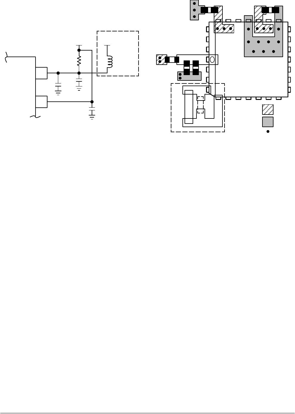
Figure 9. Power Supply Filter
PLL_V
CC
V
CC
NBC12439
NBC12439A
0.01 mF
22 mF
L=1000 mH
R=15 W
0.01 mF
3.3 V or
5.0 V
R
S
= 10−15 W
3.3 V or
5.0 V
A higher level of attenuation can be achieved by replacing
the resistor with an appropriate valued inductor. Figure 9
shows a 1000 mH choke. This value choke will show a
significant impedance at 10 KHz frequencies and above.
Because of the current draw and the voltage that must be
maintained on the PLL_V
CC
pin, a low DC resistance
inductor is required (less than 15 W). Generally, the
resistor/capacitor filter will be cheaper, easier to implement,
and provide an adequate level of supply filtering.
The NBC12439 and NBC12439A provide
sub−nanosecond output edge rates and therefore a good
power supply bypassing scheme is a must. Figure 10 shows
a representative board layout for the NBC12439. There
exists many different potential board layouts and the one
pictured is but one. The important aspect of the layout in
Figure 10 is the low impedance connections between V
CC
and GND for the bypass capacitors. Combining good quality
general purpose chip capacitors with good PCB layout
techniques will produce effective capacitor resonances at
frequencies adequate to supply the instantaneous switching
current for the NBC12439 and NBC12439A outputs. It is
imperative that low inductance chip capacitors are used. It
is equally important that the board layout not introduce any
of the inductance saved by using the leadless capacitors.
Thin interconnect traces between the capacitor and the
power plane should be avoided and multiple large vias
should be used to tie the capacitors to the buried power
planes. Fat interconnect and large vias will help to minimize
layout induced inductance and thus maximize the series
resonant point of the bypass capacitors.
Figure 10. PCB Board Layout for (PLCC−28)
C2
1
C3
R1
Xtal
C1 C1
R1 = 10−15 W
C1 = 0.01 mF
C2 = 22 mF
C3 = 0.1 mF
= V
CC
= GND
= Via
R
SHUNT
Note the dotted lines circling the crystal oscillator
connection to the device. The oscillator is a series resonant
circuit and the voltage amplitude across the crystal is
relatively small. It is imperative that no actively switching
signals cross under the crystal as crosstalk energy coupled
to these lines could significantly impact the jitter of the
device. Special attention should be paid to the layout of the
crystal to ensure a stable, jitter free interface between the
crystal and the on−board oscillator. Note the provisions for
placing a resistor across the crystal oscillator terminals as
discussed in the crystal oscillator section of this data sheet.
Although the NBC12439 and NBC12439A have several
design features to minimize the susceptibility to power
supply noise (isolated power and grounds and fully
differential PLL), there still may be applications in which
overall performance is being degraded due to system power
supply noise. The power supply filter and bypass schemes
discussed in this section should be adequate to eliminate
power supply noise−related problems in most designs.
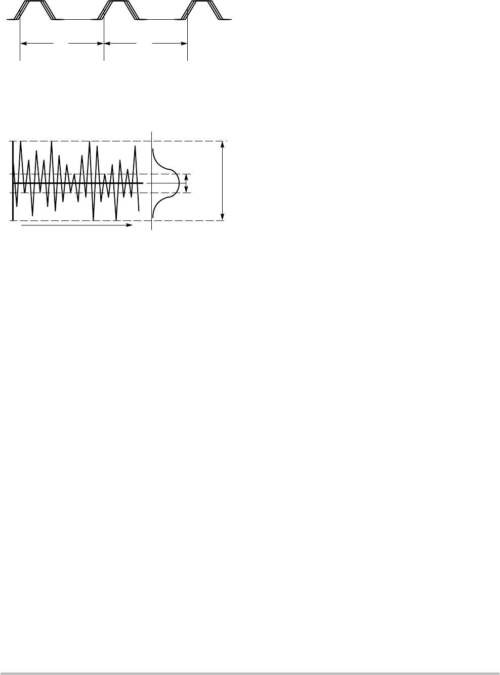
Jitter Performance
Jitter is a common parameter associated with clock
generation and distribution. Clock jitter can be defined as the
deviation in a clock’s output transition from its ideal
position.
Cycle−to−Cycle Jitter (short−term) is the period
variation between adjacent periods over a defined number of
observed cycles. The number of cycles observed is