Features
■ Lead free as standard*
■ ESD protection 30 kV max.
■ Surge protection >24 A
■ Protects 1 line
■ Uni/bidirectional confi guration
Applications
■ Computer notebooks
■ Cellular phones
■ Personal Digital Assistants (PDAs)
■ Digital cameras
Electrical & Thermal Characteristics (@ T
A
= 25 °C Unless Otherwise Noted)
CDSOD323-TxxSC - TVS Diode Series
*No lead detected in standard tests of homogeneous materials.
**RoHS Directive 2002/95/EC Jan 27, 2003 including Annex.
Specifi cations are subject to change without notice.
The device characteristics and parameters in this data sheet can and do vary in different applications and actual device performance may vary over time.
Users should verify actual device performance in their specifi c applications.
Notes:
1. Part numbers with suffi x “C” indicate bidirectional device, i.e. CDSOD323-T05SC.
2. For bidirectional devices only, the electrical specifi cations apply in both directions.
General Information
The markets of portable communications, computing and video equipment are
challenging the semiconductor industry to develop increasingly smaller electronic
components.
Bourns off ers Transient Voltage Suppressor Diodes for surge and ESD protection
applications in SOD323 package size format. The Transient Voltage Suppressor series
off ers a choice of voltage types ranging from 3 V to 36 V in a unidirectional or
bidirectional confi guration.
Bourns
®
Chip Diodes conform to JEDEC standards, are easy to handle on standard
pick and place equipment and their fl at confi guration minimizes roll away. The Bourns
®
device meets IEC 61000-4-2 (ESD), IEC 61000-4-4 (EFT) and IEC 61000-4-5 (Surge)
requirements.
Parameter Symbol Value Unit
Unidirectional Peak Pulse Power (t
p
= 8/20 μs) P
PP
500 W
Bidirectional Peak Pulse Power (t
p
= 8/20 μs) P
PP
400 W
Operating Temperature T
L
-55 to +150 ºC
Storage Temperature T
STG
-55 to +150 ºC
ESD Protection (per IEC 61000-4-2)
Contact - Min.
Contact - Max.
Air - Min.
Air - Max.
ESD
±8
±30
±15
±30
kV
Parameter Symbol
CDSOD323-
Unit
Uni-
T03S
Bi-
T03SC
Uni-
T05S
Bi-
T05SC
Uni-
T08S
Bi-
T08SC
Uni-
T12S
Bi-
T12SC
Min. Breakdown Voltage @ 1 mA V
BR
4.0 4.0 6.0 6.0 8.5 8.5 13.3 13.3 V
Working Peak Voltage V
M
3.3 3.3 5.0 5.0 8.0 8.0 12.0 12.0 V
Maximum Clamping Voltage @ I
P
= 1 A V
F
7.0 8.0 9.8 9.8 13.4 13.4 19.0 19.0 V
Typical Clamping Voltage
@ 8/20 μs @ I
PP
V
C
10.9 V
@ 43 A
10.9 V
@ 43 A
13.5 V
@ 42 A
14.5 V
@ 28 A
16.9 V
@ 34 A
18.5 V
@ 17 A
25.9 V
@ 21 A
29.5 V
@ 14 A
V
Maximum Leakage Current @ V
WM
I
D
125 125 10 10 10 10 1 1 μA
Typical Capacitance @ 0 V, 1 MHz C
P
500 200 350 175 250 150 150 50 pF
1
2
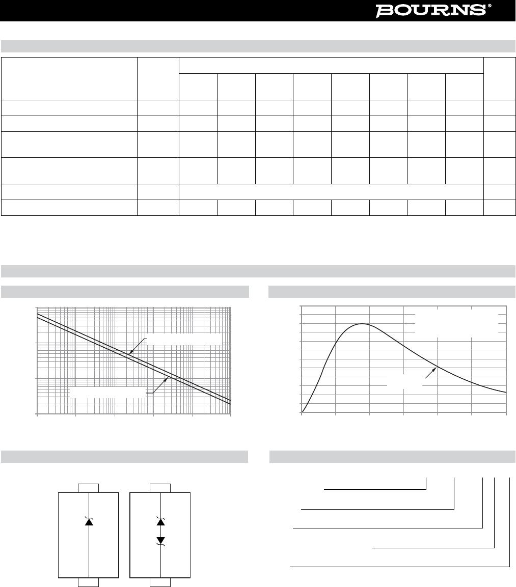
UNIDIRECTIONAL
1
2
BIDIRECTIONAL
**RoHS COMPLIANT