© 2016 Littelfuse,Inc Littelfuse.com
Specifications are subject to change without notice.
Revised July 26, 2016
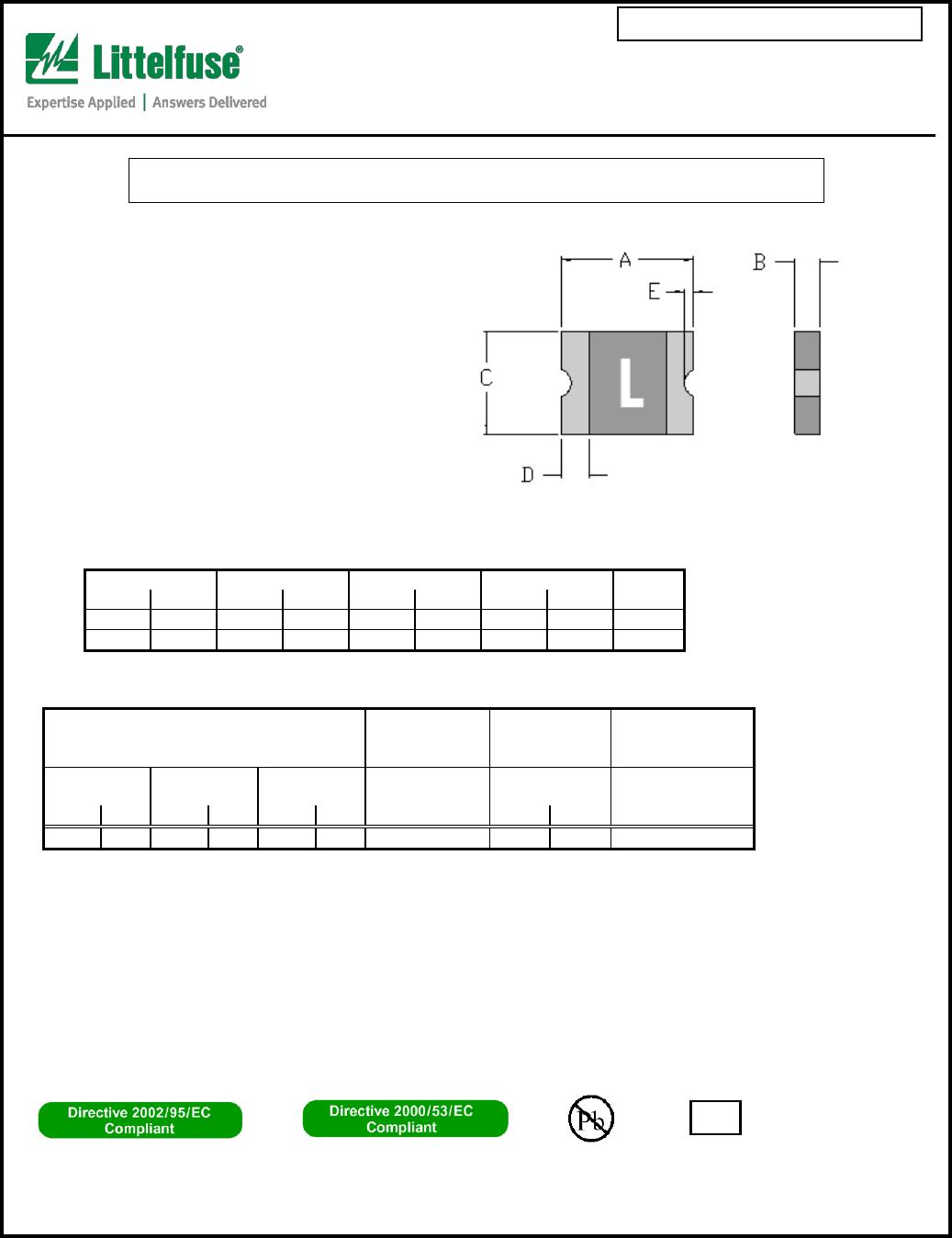
Recommended pad layout (mm.)
Recommended reflow profile
Note: All temperatures refer to top side of the package, measured on the package body surface.
Solder reflow recommendation
Recommended reflow methods: IR, hot air and Nitrogen
Recommended maximum solder paste thickness: 0.25mm
Recommended minimum stencil thickness: 0.1mm
Devices can be cleaned using standard methods and aqueous solvents.
Littelfuse believes the optimum conditions for forming acceptable solder fillets occur when a reasonable
amount of solder paste is placed underneath each device's termination. As such, we request that customers
comply with our recommended solder pad layouts.
Customer should validate that the solder paste amount and reflow recommendations meet its application.
Littelfuse requests that customer board layouts refrain from placing raised features (e.g. vias, nomenclature,
traces, etc.) underneath PolySwitch devices. It is possible that raised features could negatively impact
solderability performance of our devices.