ZL40224 Data Sheet
17
Microsemi Corporation
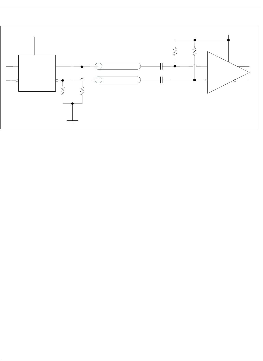
3.4 Power Supply
This device operates with either a 2.5V supply or 3.3V supply.
3.4.1 Sensitivity to power supply noise
Power supply noise from sources such as switching power supplies and high-power digital components such as
FPGAs can induce additive jitter on clock buffer outputs. The ZL40224 is equipped with a low drop out (LDO) linear
power regulator and on-chip bulk capacitors to minimize additive jitter due to power supply noise. The on-chip
regulation, recommended power supply filtering, and good PCB layout all work together to minimize the additive
jitter from power supply noise.
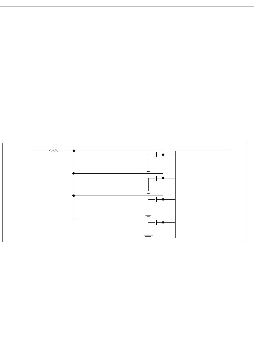
3.4.2 Power supply filtering
For optimal jitter performance, the ZL40224 should be isolated from the power planes connected to its power
supply pins as shown in Figure 20.
• 10 µF capacitors should be size 0603 or size 080
5 X5R or X7R ceramic, 6.3 V minimum rating
• 0.1 µF capacitors should be
size 0402 X5R ceramic, 6.3 V minimum rating
• Capacitors should be placed next to the
connected device power pins
Figure 20 - Decoupling Connections for Power Pins
VDD
0.15 Ohms
10 µF
0.1 µF
0.1 µF
10 µF
ZL40224
9
19
22
32
3.4.3 PCB layout considerations
The power supply filtering shown in Figure 20 can be implemented either as a plane island, or as a routed power
topology with equal results.