VNP10N06
"OMNIFET":
FULLY AUTOPROTECTED POWER MOSFET
September 2013
1
2
3
TO-220
BLOCK DIAGRAM
TYPE V
clamp
R
DS(on)
I
lim
VNP10N06 60 V 0.3 10 A
LINEAR CURRENT LIMITATION
THERMAL SHUT DOWN
SHORT CIRCUIT PROTECTION
INTEGRATED CLAMP
LOW CURRENT DRAWN FROM INPUT PIN
LOGIC LEVEL INPUT THRESHOLD
ESD PROTECTION
SCHMITT TRIGGER ON INPUT
HIGH NOISE IMMUNITY
STANDARD TO-220 PACKAGE
DESCRIPTION
The VNP10N06 is a monolithic device made
using STMicroelectronics VIPower Technology,
intended for replacement of standard power
MOSFETS in DC to 50 KHz applications.
Built-in thermal shut-down, linear current limi-
tation and overvoltage clamp protect the chip
n harsh enviroments.
1/11
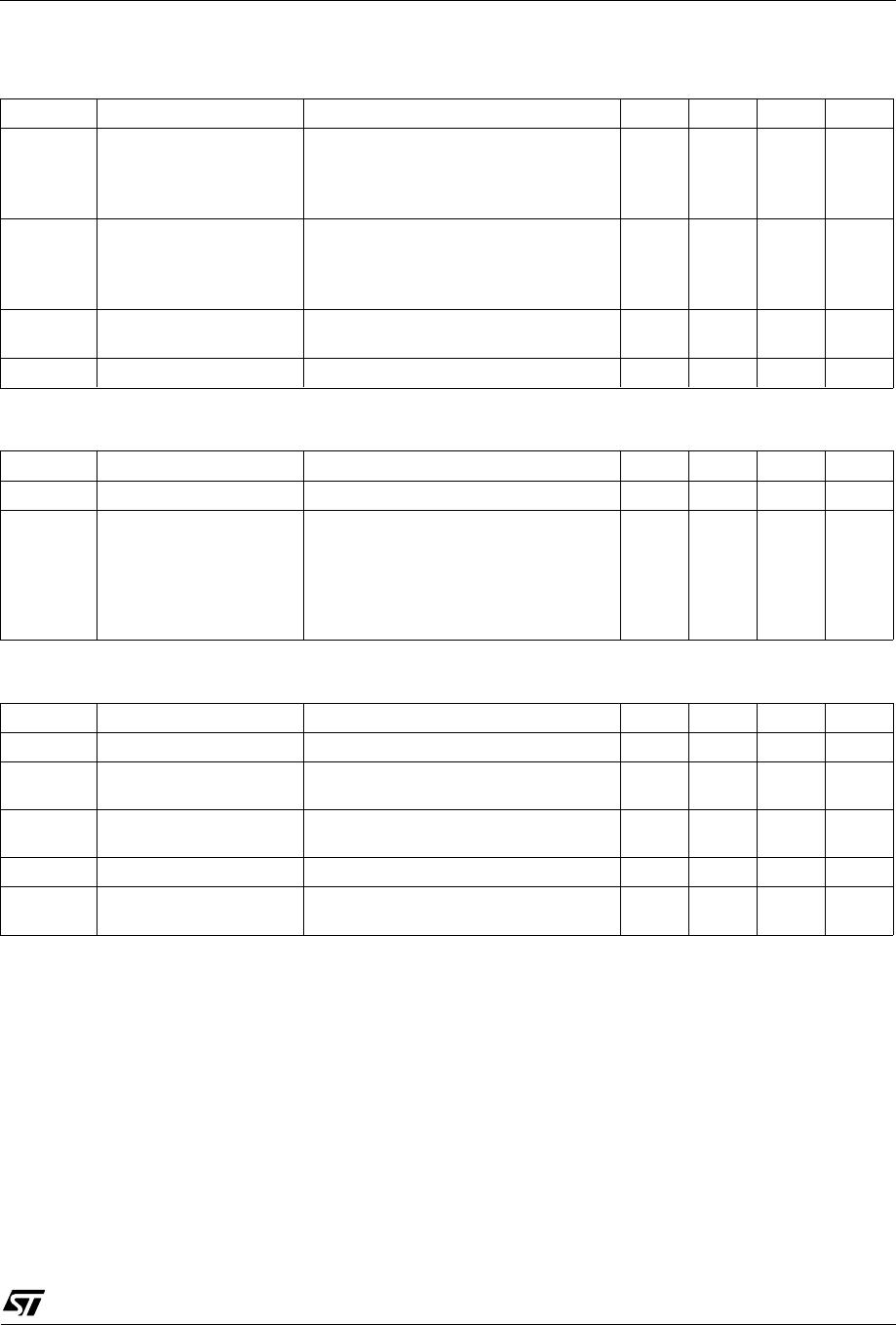
ABSOLUTE MAXIMUM RATING
Symbol Parameter Value Unit
V
DS
Drain-source Voltage (V
in
= 0) Internally Clamped V
V
in
Input Voltage Internally Clamped V
I
in
Input Current ± 20 mA
I
D
Drain Current Internally Limited A
I
R
Reverse DC Output Current -15 A
V
esd
Electrostatic Discharge (C= 100 pF, R=1.5 K)
4000 V
P
tot
Total Dissipation at T
c
= 25
o
C42W
T
j
Operating Junction Temperature Internally Limited
o
C
T
c
Case Operating Temperature Internally Limited
o
C
T
stg
Storage Temperature -55 to 150
o
C
THERMAL DATA
R
thj-case
R
thj-amb
Thermal Resistance Junction-case Max
Thermal Resistance Junction-ambient Max
3
62.5
o
C/W
o
C/W
ELECTRICAL CHARACTERISTICS (T
case
= 25
o
C unless otherwise specified)
OFF
Symbol Parameter Test Conditions Min. Typ. Max. Unit
V
CLAMP
Drain-source Clamp
Voltage
I
D
= 200 mA V
in
= 0 506070 V
V
IL
Input Low Level
Voltage
I
D
= 100 µA V
DS
= 16 V
1.5 V
V
IH
Input High Level
Voltage
R
L
= 27 V
DD
= 16 V
V
DS
= 0.5 V
3.2 V
V
INCL
Input-Source Reverse
Clamp Voltage
I
in
= -1 mA
I
in
= 1 mA
-1
8
-0.3
11
V
V
I
DSS
Zero Input Voltage
Drain Current (V
in
= 0)
V
DS
= 50 V V
in
= V
IL
V
DS
< 35 V V
in
= V
IL
250
100
µA
µA
I
ISS
Supply Current from
Input Pin
V
DS
= 0 V V
in
= 5 V 150 300 µA
ON ()
Symbol Parameter Test Conditions Min. Typ. Max. Unit
R
DS(on)
Static Drain-source On
Resistance
V
in
= 7 V I
D
= 1 A T
J
< 125
o
C
0.15 0.3
DYNAMIC
Symbol Parameter Test Conditions Min. Typ. Max. Unit
C
oss
Output Capacitance V
DS
= 13 V f = 1 MHz V
in
= 0 350 500 pF
VNP10N06
2/11
ELECTRICAL CHARACTERISTICS (continued)
SWITCHING (∗∗)
Symbol Parameter Test Conditions Min. Typ. Max. Unit
t
d(on)
t
r
t
d(off)
t
f
Turn-on Delay Time
Rise Time
Turn-off Delay Time
Fall Time
V
DD
= 16 V I
d
= 1 A
V
gen
= 7 V R
gen
= 10
(see figure 3)
1100
550
200
100
1600
900
400
200
ns
ns
ns
ns
t
d(on)
t
r
t
d(off)
t
f
Turn-on Delay Time
Rise Time
Turn-off Delay Time
Fall Time
V
DD
= 16 V I
d
= 1 A
V
gen
= 7 V R
gen
= 1000
(see figure 3)
1.2
1
1.6
1.2
1.8
1.5
2.3
1.8
µs
µs
µs
µs
(di/dt)
on
Turn-on Current Slope V
DD
= 16 V I
D
= 1 A
V
in
= 7 V R
gen
= 10
1.5 A/µs
Q
i
Total Input Charge V
DD
= 12 V I
D
= 1 A V
in
= 7 V 13 nC
SOURCE DRAIN DIODE
Symbol Parameter Test Conditions Min. Typ. Max. Unit
V
SD
() Forward On Voltage I
SD
= 1 A V
in
= V
IL
0.8 1.6 V
t
rr
(∗∗)
Q
rr
(∗∗)
I
RRM
(∗∗)
Reverse Recovery
Time
Reverse Recovery
Charge
Reverse Recovery
Current
I
SD
= 1 A di/dt = 100 A/µs
V
DD
= 30 V T
j
= 25
o
C
(see test circuit, figure 5)
125
0.22
3.5
ns
µC
A
PROTECTION
Symbol Parameter Test Conditions Min. Typ. Max. Unit
I
lim
Drain Current Limit V
in
= 7 V V
DS
= 13 V 6 10 15 A
t
dlim
(∗∗) Step Response
Current Limit
V
in
= 7 V V
DS
step from 0 to 13 V 12 20 µs
T
jsh
(∗∗) Overtemperature
Shutdown
150
o
C
T
jrs
(∗∗) Overtemperature Reset 135
o
C
E
as
(∗∗) Single Pulse
Avalanche Energy
starting T
j
= 25
o
C V
DD
= 24 V
V
in
= 7 V R
gen
= 1 K L = 10 mH
250 mJ
() Pulsed: Pulse duration = 300 µs, duty cycle 1.5 %
(∗∗) Parameters guaranteed by design/characterization
VNP10N06
3/11

VNP10N06-E

Mfr. #:
Manufacturer:
STMicroelectronics
Description:
MOSFET N-Ch 60V 10A OmniFET
Lifecycle:
New from this manufacturer.
Delivery:
DHL FedEx Ups TNT EMS
Payment:
T/T Paypal Visa MoneyGram Western Union

Products related to this Datasheet