Data Sheet ADuM2210/ADuM2211
Rev. F | Page 13 of 17
APPLICATIONS INFORMATION
PCB LAYOUT
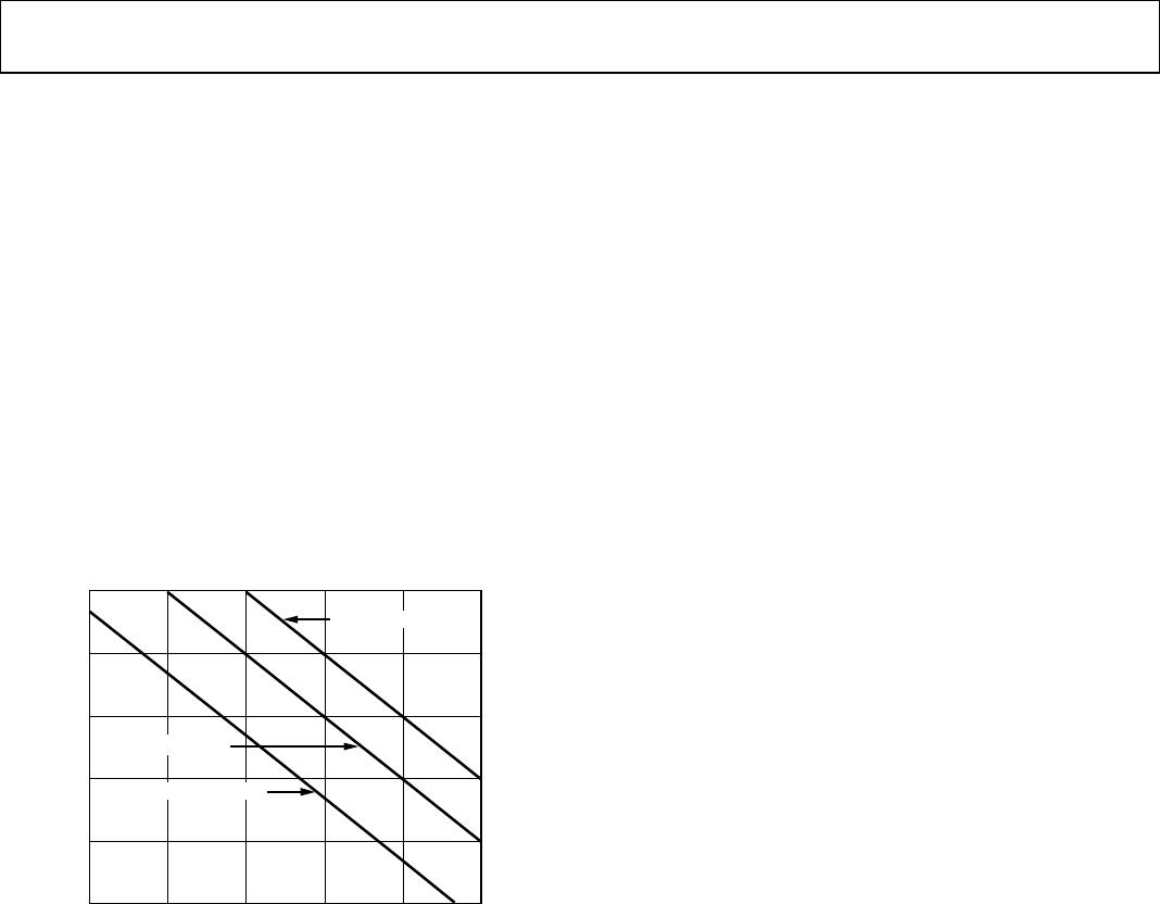
The ADuM2210/ADuM2211 digital isolator requires no external
interface circuitry for the logic interfaces. Power supply bypassing
is strongly recommended at the input and output supply pins
(see Figure 12). Bypass capacitors are most conveniently connected
between Pin 1 and Pin 3 for V
DD1
and between Pin 14 and Pin 16
for V
DD2
. The capacitor value should be between 0.01 μF and 0.1 μF.
The total lead length between both ends of the capacitor and
the input power supply pin should not exceed 20 mm. Bypassing
between Pin 3 and Pin 7 and between Pin 9 and Pin 14 should
be considered unless the ground pair on each package side is
connected close to the package.
GND
1
NC
V
DD1
V
IA
/V
OA
GND
2
NC
V
DD2
V
OA
/V
IA
V
IB
V
OB
NC
NC
GND
1
NC
NC
GND
2
09233-012
Figure 12. Recommended Printed Circuit Board Layout
In applications involving high common-mode transients, care
should be taken to ensure that board coupling across the isolation
barrier is minimized. Furthermore, the board layout should be
designed such that any coupling that does occur equally affects
all pins on a given component side. Failure to ensure this could
cause voltage differentials between pins exceeding the Absolute
Maximum Ratings of the device, thereby leading to latch-up or
permanent damage.
See the AN-1109 Application Note for board layout guidelines.
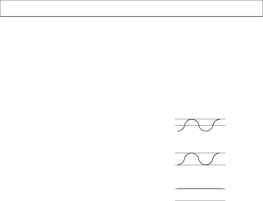
PROPAGATION DELAY-RELATED PARAMETERS
Propagation delay is a parameter that describes the length of
time it takes for a logic signal to propagate through a component.
The propagation delay to a logic low output can differ from the
propagation delay to logic high.
INPUT (
Ix
)
OUTPUT (V
Ox
)
t
PLH
t
PHL
50%
50%
09233-013
Figure 13. Propagation Delay Parameters
Pulse width distortion is the maximum difference between these
two propagation delay values and is an indication of how
accurately the input signal’s timing is preserved.
Channel-to-channel matching refers to the maximum amount
the propagation delay differs among channels within a single
ADuM2210/ADuM2211 component.
Propagation delay skew refers to the maximum amount the
propagation delay differs among multiple ADuM2210/ADuM2211
components operated under the same conditions.
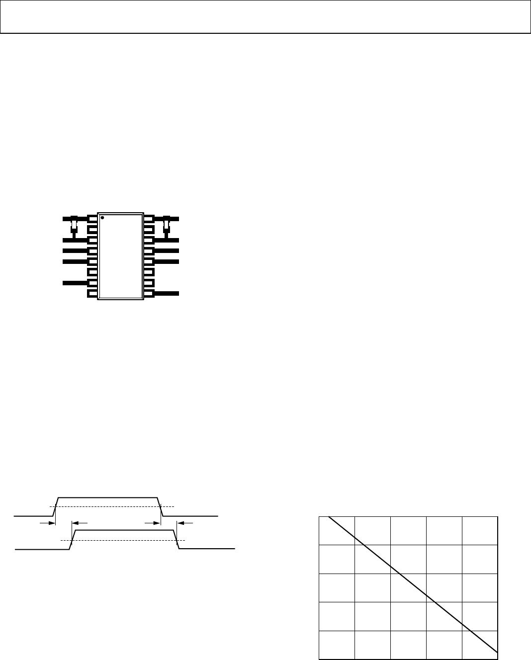
DC CORRECTNESS AND MAGNETIC FIELD
IMMUNITY
Positive and negative logic transitions at the isolator input cause
narrow (~1 ns) pulses to be sent via the transformer to the
decoder. The decoder is bistable and is, therefore, either set or
reset by the pulses, indicating input logic transitions. In the
absence of logic transitions at the input for more than ~1 μs, a
periodic set of refresh pulses indicative of the correct input state
is sent to ensure dc correctness at the output. If the decoder
receives no internal pulses for more than approximately 5 μs,
the input side is assumed to be without power or nonfunctional;
in which case, the isolator output is forced to a default state (see
Table 20 and Table 21) by the watchdog timer circuit.
The limitation on the ADuM2210/ADuM2211 magnetic field
immunity is set by the condition in which induced voltage in the
transformer receiving coil is large enough to either falsely set or
reset the decoder. The following analysis defines the conditions
under which this can occur. The 3.3 V operating condition of
the ADuM2210/ADuM2211 is examined because it represents
the most susceptible mode of operation.
The pulses at the transformer output have an amplitude greater
than 1.0 V. The decoder has a sensing threshold at about 0.5 V,
therefore establishing a 0.5 V margin in which induced voltages
can be tolerated. The voltage induced across the receiving coil is
given by
V = (−dβ/dt)Σπr
n
2
; n = 1, 2,…, N
where:
β is the magnetic flux density (gauss).
N is the number of turns in the receiving coil.
r
n
is the radius of the n
th
turn in the receiving coil (cm).
Given the geometry of the receiving coil in the ADuM2210/
ADuM2211 and an imposed requirement that the induced
voltage be at most 50% of the 0.5 V margin at the decoder, a
maximum allowable magnetic field is calculated as shown in
Figure 14.
MAGNETIC FIELD FREQUENCY (Hz)
100
MAXIMUM ALLOWABLE MAGNETIC FLUX
DENSITY (kgauss)
0.001
1M
10
0.01
1k 10k 10M
0.1
1
100M100k
09233-014
Figure 14. Maximum Allowable External Magnetic Flux Density