VBUS54CV-HSF
www.vishay.com
Vishay Semiconductors
Rev. 1.1, 16-Jul-15
2
Document Number: 84145
For technical questions, contact: ESDprotection@vishay.com
THIS DOCUMENT IS SUBJECT TO CHANGE WITHOUT NOTICE. THE PRODUCTS DESCRIBED HEREIN AND THIS DOCUMENT
ARE SUBJECT TO SPECIFIC DISCLAIMERS, SET FORTH AT www.vishay.com/doc?91000
APPLICATION NOTE
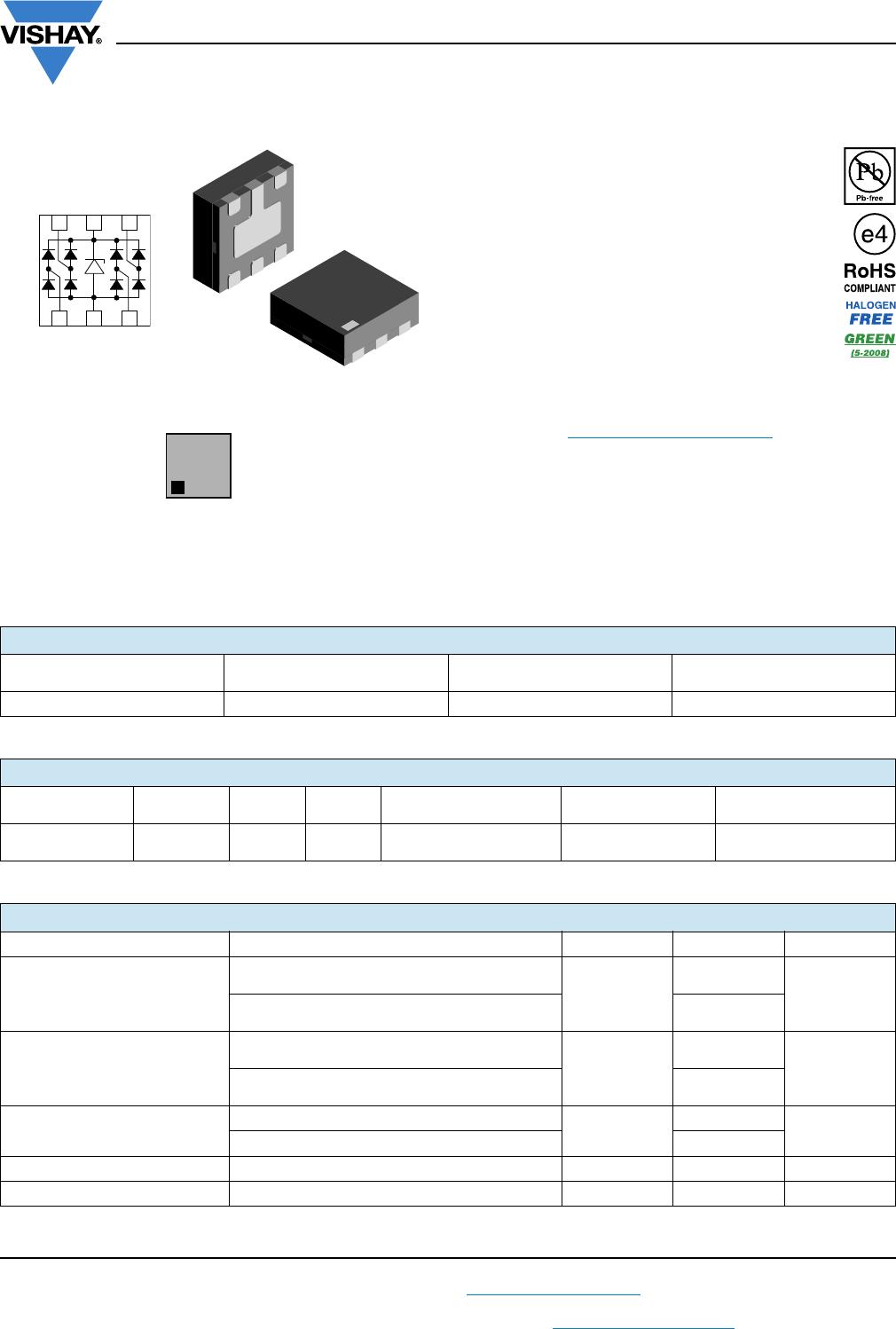
With the VBUS54CV-HSF a double, high speed USB-port can be protected against transient voltage signals. Negative
transients will be clamped close below the ground level while positive transients will be clamped close above the working range.
An avalanche diode clamps the supply line (V
BUS
at pin 5) to ground (pin 2). The high speed data lines, D
1+
, D
2+
, D
1-
and D
2-
,
are connected to pin 1, 3, 4 and 6. As long as the signal voltage on the data lines is between the ground- and the V
BUS
-level,
the low capacitance PN-diodes offer a very high isolation to V
BUS
, ground and to the other data lines. But as soon as any
transient signal exceeds this working range, one of the PN-diodes gets in the forward mode and clamps the transient to ground
or the avalanche break through voltage level.
ELECTRICAL CHARACTERISTICS VBUS54CV-HSF (pin 1, 3, 4, or 6 to pin 2)
(T
amb
= 25 °C, unless otherwise specified)
PARAMETER TEST CONDITIONS/REMARKS SYMBOL MIN. TYP. MAX. UNIT
Protection paths Number of lines which can be protected N
channel
- - 4 lines
Reverse stand-off voltage Max. reverse working voltage V
RWM
--5.5V
Reverse voltage at I
R
= 0.1 μA V
R
5.5 - - V
Reverse current at V
RWM
= 5.5 V I
R
- 0.01 0.1 μA
Reverse breakdown voltage at I
R
= 1 mA V
BR
77.98.6V
Reverse clamping voltage at I
PP
= 11 A V
C
-1822V
Forward clamping voltage at I
PP
=11 A V
F
-6.58 V
Capacitance
V
R
(at I/O pin) = 0 V
V
R
(at pin 5) = 5 V; f = 1 MHz
C
D
-1.22.5pF
Line symmetry Difference of the line capacitances dC
D
--0.2pF
ELECTRICAL CHARACTERISTICS (pin 5 to pin 2)
(T
amb
= 25 °C, unless otherwise specified)
PARAMETER TEST CONDITIONS/REMARKS SYMBOL MIN. TYP. MAX. UNIT
Reverse stand-off voltage Max. reverse working voltage V
RWM
--5.5V
Reverse voltage at I
R
= 0.1 μA; pin 2 to pin 1 V
R
5.5 - - V
Reverse current at V
RWM
= 5.5 V I
R
- 0.01 0.1 μA
Reverse breakdown voltage at I
R
= 1 mA V
BR
6.3 7.1 8 V
Reverse clamping voltage at I
PP
= 13 A V
C
-1822V
Forward clamping voltage at I
PP
=13 A V
F
--7V
Capacitance V
R
(at pin 5) = 0 V; f = 1 MHz C
D
- 190 - pF
R
E
C
E
I
V
E
R
IC
20399
6
4
5
1
2
3
t
i
w
n
U
S
B
-
P
o
r
t
V
BUS
D
1+
D
1-
D
2+
D
2-
G
ND