Ultralow Noise
Drivers for Low Voltage ADCs
Data Sheet ADA4930-1/ADA4930-2
Rev. B Document Feedback
Information furnished by Analog Devices is believed to be accurate and reliable. However, no
responsibility is assumed by Analog Devices for its use, nor for any infringements of patents or other
rights of third parties that may result from its use. Specifications subject to change without notice. No
license is granted by implication or otherwise under any patent or patent rights of Analog Devices.
Trademarks and registered trademarks are the property of their respective owners.
One Technology Way, P.O. Box 9106, Norwood, MA 02062-9106, U.S.A.
Tel: 781.329.4700 ©2010–2015 Analog Devices, Inc. All rights reserved.
Technical Support www.analog.com
FEATURES
Low input voltage noise: 1.2 nV/√Hz
Low common-mode output: 0.9 V on single supply
Extremely low harmonic distortion
−104 dBc HD2 at 10 MHz
−79 dBc HD2 at 70 MHz
−73 dBc HD2 at 100 MHz
−101 dBc HD3 at 10 MHz
−82 dBc HD3 at 70 MHz
−75 dBc HD3 at 100 MHz
High speed
−3 dB bandwidth of 1.35 GHz, G = 1
Slew rate: 3400 V/μs, 25% to 75%
0.1 dB gain flatness to 380 MHz
Fast overdrive recovery of 1.5 ns
0.5 mV typical offset voltage
Externally adjustable gain
Differential-to-differential or single-ended-to-differential
operation
Adjustable output common-mode voltage
Single-supply operation: 3.3 V or 5 V
APPLICATIONS
ADC drivers
Single-ended-to-differential converters
IF and baseband gain blocks
Differential buffers
Line drivers
GENERAL DESCRIPTION
The ADA4930-1/ADA4930-2 are very low noise, low distortion,
high speed differential amplifiers. They are an ideal choice for
driving 1.8 V high performance ADCs with resolutions up to
14 bits from dc to 70 MHz. The adjustable output common
mode allows the ADA4930-1/ADA4930-2 to match the input of
the ADC. The internal common-mode feedback loop provides
exceptional output balance, suppression of even-order harmonic
distortion products, and dc level translation.
With the ADA4930-1/ADA4930-2, differential gain configurations
are easily realized with a simple external feedback network of
four resistors determining the closed-loop gain of the amplifier.
The ADA4930-1/ADA4930-2 are fabricated using Analog
Devices, Inc., proprietary silicon-germanium (SiGe), comple-
mentary bipolar process, enabling them to achieve very low
levels of distortion with an input voltage noise of only 1.2 nV/√Hz.
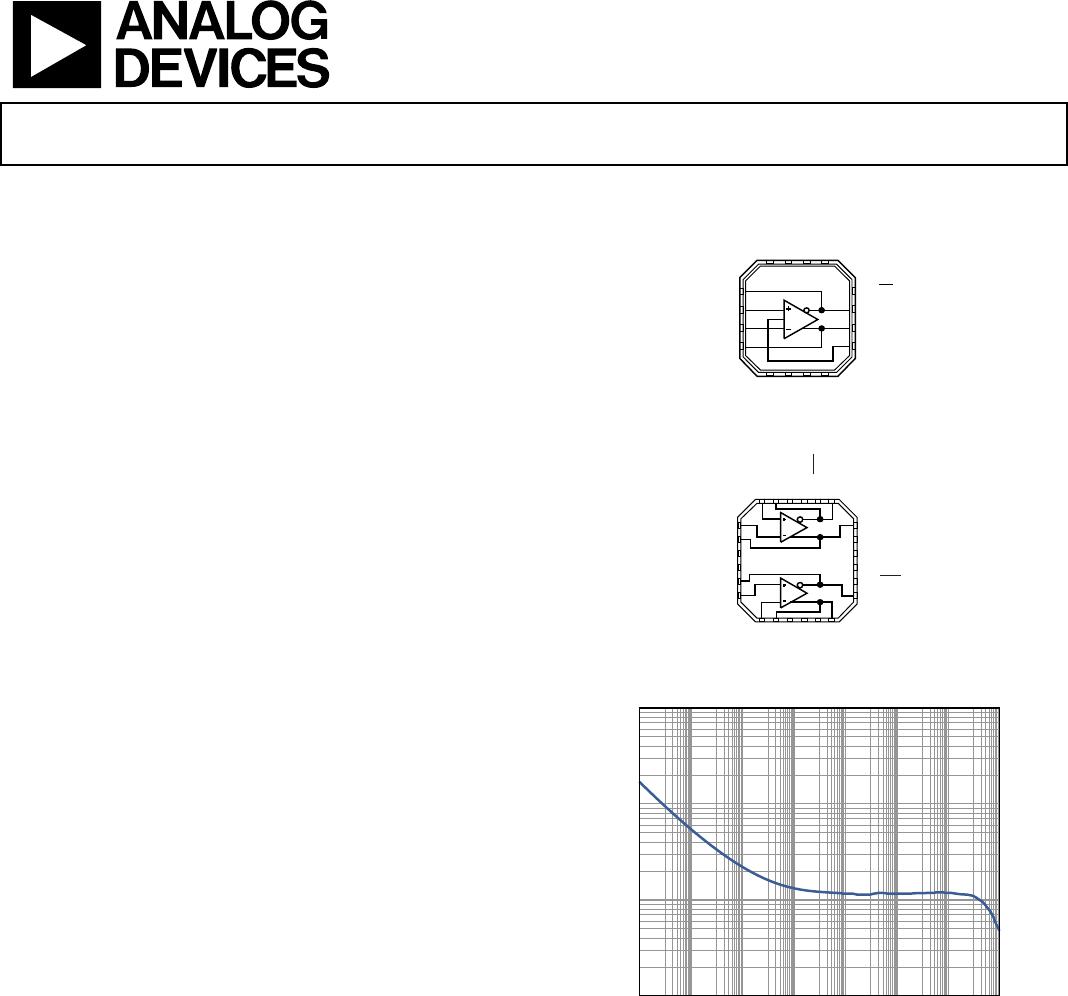
FUNCTIONAL BLOCK DIAGRAMS
1–FB
2+IN
3–IN
4+FB
11 –OUT
12 PD
10 +OUT
9V
OCM
5
+V
S
6
+V
S
7
+V
S
8
+V
S
15
–V
S
16
–V
S
14
–V
S
13
–V
S
ADA4930-1
09209-001
Figure 1.
ADA4930-2
1–IN1
2+FB1
3+V
S1
4+V
S1
5–FB2
6+IN2
15
–V
S2
16 –V
S2
17 V
OCM1
18 +OUT1
14
PD2
13 –OUT2
7
–IN2
8
+FB2
9
+V
S2
11
V
OCM
2
12
+OUT2
10
+V
S2
21
–V
S1
22
–V
S1
23
–FB1
24
+IN1
20
PD1
19
–OUT1
09209-002
Figure 2.
0
1
10
100
10 100 1k 10k 100k 1M 10M 100M
V
N
(nV/
hz)
FREQUENCY (Hz)
09209-003
Figure 3. Voltage Noise Spectral Density
The low dc offset and excellent dynamic performance of the
ADA4930-1/ADA4930-2 make them well suited for a wide
variety of data acquisition and signal processing applications.
The ADA4930-1 is available in a Pb-free, 3 mm × 3 mm 16-lead
LFCSP, and the ADA4930-2 is available in a Pb-free, 4 mm × 4 mm
24-lead LFCSP. The pinout has been optimized to facilitate printed
circuit board (PCB) layout and minimize distortion. The
ADA4930-1 is specified to operate over the −40°C to +105°C
temperature range, and the ADA4930-2 is specified to operate over
the −40°C to +105°C temperature range for 3.3 V or 5 V supply
voltages.
ADA4930-1/ADA4930-2 Data Sheet
Rev. B | Page 2 of 25
TABLE OF CONTENTS
Features .............................................................................................. 1
Applications ....................................................................................... 1
General Description ......................................................................... 1
Functional Block Diagrams ............................................................. 1
Revision History ............................................................................... 2
Specifications ..................................................................................... 3
3.3 V Operation ............................................................................ 3
3.3 V V
OCM
to V
O, cm
Performance ............................................... 4
3.3 V General Performance ......................................................... 4
5 V Operation ............................................................................... 5
5 V V
OCM
to V
O, cm
Performance .................................................. 6
5 V General Performance ............................................................ 6
Absolute Maximum Ratings ............................................................ 7
Thermal Resistance ...................................................................... 7
Maximum Power Dissipation ..................................................... 7
ESD Caution .................................................................................. 7
Pin Configurations and Function Descriptions ........................... 8
Typical Performance Characteristics ............................................. 9
Test Circuits ..................................................................................... 15
Operational Description ................................................................ 16
Definition of Terms .................................................................... 16
Theory of Operation ...................................................................... 17
Analyzing an Application Circuit ............................................ 17
Setting the Closed-Loop Gain .................................................. 17
Estimating the Output Noise Voltage ...................................... 17
Impact of Mismatches in the Feedback Networks ................. 18
Input Common-Mode Voltage Range ..................................... 18
Minimum R
G
Value .................................................................... 19
Setting the Output Common-Mode Voltage .......................... 19
Calculating the Input Impedance for an Application Circuit ..... 19
Layout, Grounding, and Bypassing .............................................. 23
High Performance ADC Driving ................................................. 24
Outline Dimensions ....................................................................... 25
Ordering Guide .......................................................................... 25
REVISION HISTORY
1/15—Rev. A to Rev. B
Updated Outline Dimensions ....................................................... 25
Changes to Ordering Guide .......................................................... 25
10/10—Rev. 0 to Rev. A
Changes to General Description Section ...................................... 1
10/10—Revision 0: Initial Version
Data Sheet ADA4930-1/ADA4930-2
Rev. B | Page 3 of 25
SPECIFICATIONS
3.3 V OPERATION
V
S
= 3.3 V, V
ICM
= 0.9 V, V
OCM
= 0.9 V, R
F
= 301 Ω, R
G
= 301 Ω, R
L, dm
= 1 kΩ, single-ended input, differential output, T
A
= 25°C, T
MIN
to
T
MAX
= −40°C to +105°C, unless otherwise noted.
Table 1.
Parameter Test Conditions/Comments Min Typ Max Unit
DYNAMIC PERFORMANCE
−3 dB Small Signal Bandwidth V
O, dm
= 0.1 V p-p 1430 MHz
−3 dB Large Signal Bandwidth V
O, dm
= 2 V p-p 887 MHz
Bandwidth for 0.1 dB Flatness V
O, dm
= 0.1 V p-p
ADA4930-1 380 MHz
ADA4930-2 89 MHz
Slew Rate V
O, dm
= 2 V step, 25% to 75% 2877 V/μs
Settling Time to 0.1% V
O, dm
= 2 V step, R
L
= 200 Ω 6.3 ns
Overdrive Recovery Time G = 3, V
IN, dm
= 0.7 V p-p pulse 1.5 ns
NOISE/HARMONIC PERFORMANCE
HD2/HD3 V
O, dm
= 2 V p-p, f
C
= 10 MHz −98/−97 dB
V
O, dm
= 2 V p-p, f
C
= 30 MHz −91/−88 dB
V
O, dm
= 2 V p-p, f
C
= 70 MHz −79/−79 dB
V
O, dm
= 2 V p-p, f
C
= 100 MHz −73/−73 dB
Third-Order IMD V
O, dm
= 1 V p-p/tone, f
C
= 70.05 MHz ± 0.05 MHz 91 dBc
V
O, dm
= 1 V p-p/tone, f
C
= 140.05 MHz ± 0.05 MHz 86 dBc
Input Voltage Noise f = 100 kHz 1.15 nV/√Hz
Input Current Noise f = 100 kHz 3 pA/√Hz
Crosstalk f = 100 MHz, ADA4930-2, R
L
= 200 Ω −90 dB
DC PERFORMANCE
Input Offset Voltage V
IP
= V
IN
= V
OCM
= 0 V, R
L
= open circuit
−3.1 −0.5 +3.1 mV
Input Offset Voltage Drift T
MIN
to T
MAX
2.75 μV/°C
Input Bias Current −36 −24 −16 μA
Input Bias Current Drift T
MIN
to T
MAX
−0.05
μA/C
Input Offset Current −1.8 +0.1 +1.8 μA
Open-Loop Gain R
F
= R
G
= 10 kΩ, ΔV
O
= 0.5 V, R
L
= open circuit 64 dB
INPUT CHARACTERISTICS
Input Common-Mode Voltage Range 0.3 1.2 V
Input Resistance Differential 150
Common mode 3
Input Capacitance Common mode 1 pF
CMRR ΔV
ICM
= 0.5 V dc; R
F
= R
G
= 10 kΩ, R
L
= open circuit −82 −77 dB
OUTPUT CHARACTERISTICS
Output Voltage Each single-ended output; R
F
= R
G
= 10 kΩ 0.11 1.74 V
Linear Output Current Each single-ended output; f = 1 MHz, TDH ≤ 60 dBc 30 mA
Output Balance Error f = 1 MHz 55 dB

ADA4930-2YCPZ-RL

Mfr. #:
Manufacturer:
Analog Devices Inc.
Description:
Differential Amplifiers Ultralow Noise Dvrs for Low VTG ADC's
Lifecycle:
New from this manufacturer.
Delivery:
DHL FedEx Ups TNT EMS
Payment:
T/T Paypal Visa MoneyGram Western Union