ICS2304NZ-1
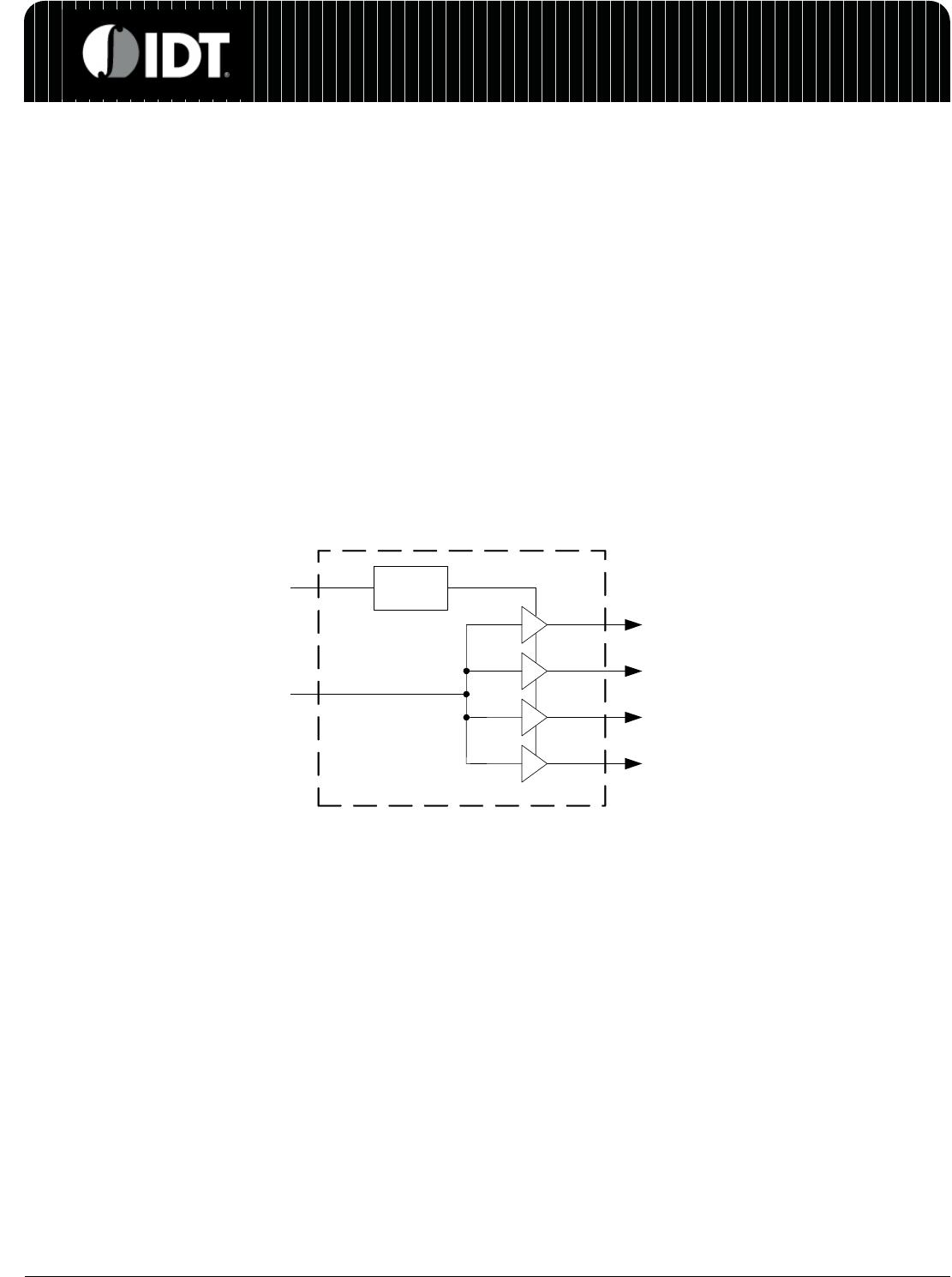
LOW SKEW PCI/PCI-X BUFFER FAN OUT BUFFER
IDT®
LOW SKEW PCI/PCI-X BUFFER 3
ICS2304NZ-1 REV G 110110
Absolute Maximum Ratings
Stresses above the ratings listed below can cause permanent damage to the ICS2304NZ-1. These ratings, which
are standard values for IDT commercially rated parts, are stress ratings only. Functional operation of the device at
these or any other conditions above those indicated in the operational sections of the specifications is not implied.
Exposure to absolute maximum rating conditions for extended periods can affect product reliability. Electrical
parameters are guaranteed only over the recommended operating temperature range.
Notes:
1. The input and output negative-voltage ratings may be exceeded if the input and output clamp-current ratings are
observed.
2. This value is limited to 4.6 V maximum.
3. The package thermal impedance is calculated in accordance with JESD 51.
Recommended Operation Conditions
Timing Requirements Over Recommended Ranges of Supply Voltage and Operating Free-air
Temperature
Item Rating
Supply Voltage Range, V
DD
-0.5 V to 4.3 V
Input Voltage Range, V
I
(see notes 1 and 2) -0.5 V to V
DD
+ 0.5 V
Output Voltage Range, V
O
(see notes 1 and 2) -0.5 V to V
DD
+ 0.5 V
Input Clamp Current, I
IK
(V
I
<0 or V
I
>V
DD
)±50 mA
Output Clamp Current, I
IK
(V
O
<0 or V
O
)±50 mA
Continuous Total Output Current, I
O
(V
O
= 0 to V
DD
)±50 mA
Package Thermal Impedance, θ
JA
(see note 3): PW
Package
230.5° C/W
Storage Temperature Range, T
stg
-65° C to 150° C
Parameter Min. Typ. Max. Units
Supply Voltage, V
DD
33.33.6V
High-level Input Voltage, V
IH
0.7 x V
DD
V
Low-level Input Voltage, V
IL
0.3 x V
DD
V
Input Voltage, V
I
0V
DD
V
High-level Output Current, I
OH
-24 mA
Low-level Output Current, I
OL
24 mA
Operating Free-air Temperature, T
A
-40 – +85 ° C
Min. Typ. Max. Units
Clock Frequency, f
CLK
0 140 MHz