JCK1524D05

DCDC
Specification
15 Watts
2:1 Input Range
Industry Standard Package
1500 VDC Isolation
Continuous Short Circuit Protection
High Efficiency up to 89%
40 °C to +100 °C Operating Temperature
3 Year Warranty
JCK Series
Input
Input Voltage Range 12 V (9-18 VDC)
24 V (18-36 VDC)
48 V (36-75 VDC)
Input Current See table
Input Reflected 20 mA rms through 12 µH inductor,
Ripple Current 5 Hz to 20 MHz
Under Voltage Lockout 12 V models On 8.6 V, Off 7.9 V typical
24 V models On 17.8 V, Off 16 V typical
48 V models On 33.5 V, Off 30.5 V typical
Input Surge 12 V models 30 VDC for 100 ms
24 V models 50 VDC for 100 ms
48 V models 100 VDC for 100 ms
Output
Output Voltage See table
Minimum Load No minimum load required
Line Regulation ±0.5% max
Load Regulation ±0.5% max for single and dual outputs
except ±0.8% for D03 versions
Cross Regulation ±5% max on dual output models
(see note 2)
Setpoint Accuracy ±1.0% max
Start Up Delay <20 ms
Start Up Rise Time <5 ms
Ripple & Noise 75 mV pk-pk max (see note 3)
Transient Response ±3% max deviation, recovery to within 1%
in 250 µs for a 25% load change
Temperature 0.02%/°C
Coefficient
Overload Protection >140% of full load at nominal input
Short Circuit Protection Trip & restart (hiccup mode) with
auto recovery
Maximum Capacitive See table
Load
xppower.com
General
Efficiency See table
Isolation Voltage 1600 VDC Input to Output,
optional 3500 V (see note 4)
1600 VDC Input to Case
1600 VDC Output to Case
Isolation Capacitance 1200 pF typical
Isolation Resistance 10
9
Ω min
Switching Frequency 300 kHz typical
Power Density 18.75 W/in
3
MTBF >1.1 MHrs to MIL-HDBK-217F
at 25 °C, GB
Environmental
Operating Temperature -40 °C to +100 °C, derate from 100% load
at +70 °C to 0% load at +100 °C
Case Temperature +100 °C max
Storage Temperature -40 °C to +125 °C
Cooling Convection-cooled
Operating Humidity Up to 95% RH, non-condensing
EMC
Emissions EN55022, Class A conducted
& radiated with external components,
see application note
ESD Immunity EN61000-4-2, 8 kV air, 6 kV contact,
Perf Criteria A
Radiated Immunity EN61000-4-3 10 V/m, Perf Criteria A
EFT/Burst EN61000-4-4 level 3, Perf Criteria B*
Surge EN61000-4-5 level 2, Perf Criteria B*
Conducted Immunity EN61000-4-6 10 V/rms,Perf Criteria A
Magnetic Field EN61000-4-8 1 A/m, Perf Criteria A
*External input capacitor required 220 µF/100 V.
1.00
(25.40)
2.00
(50.80)
0.60
(15.24)
0.80
(20.32)
0.60
(15.24)
0.40
(10.16)
0.20
(5.08)
0.40
(10.16)
0.10
(2.54)
0.40
(10.16)
0.40
(10.16)
0.10
(2.54)
34
12
5
Bottom View
0.40
(10.16)
DIA.
0.04
(1.00)
0.20
(5.08)
min
Thermal Pad
2.00
(50.80)
0.64
(16.3)
Optional heatsink (-HK)
DCDC
JCK15
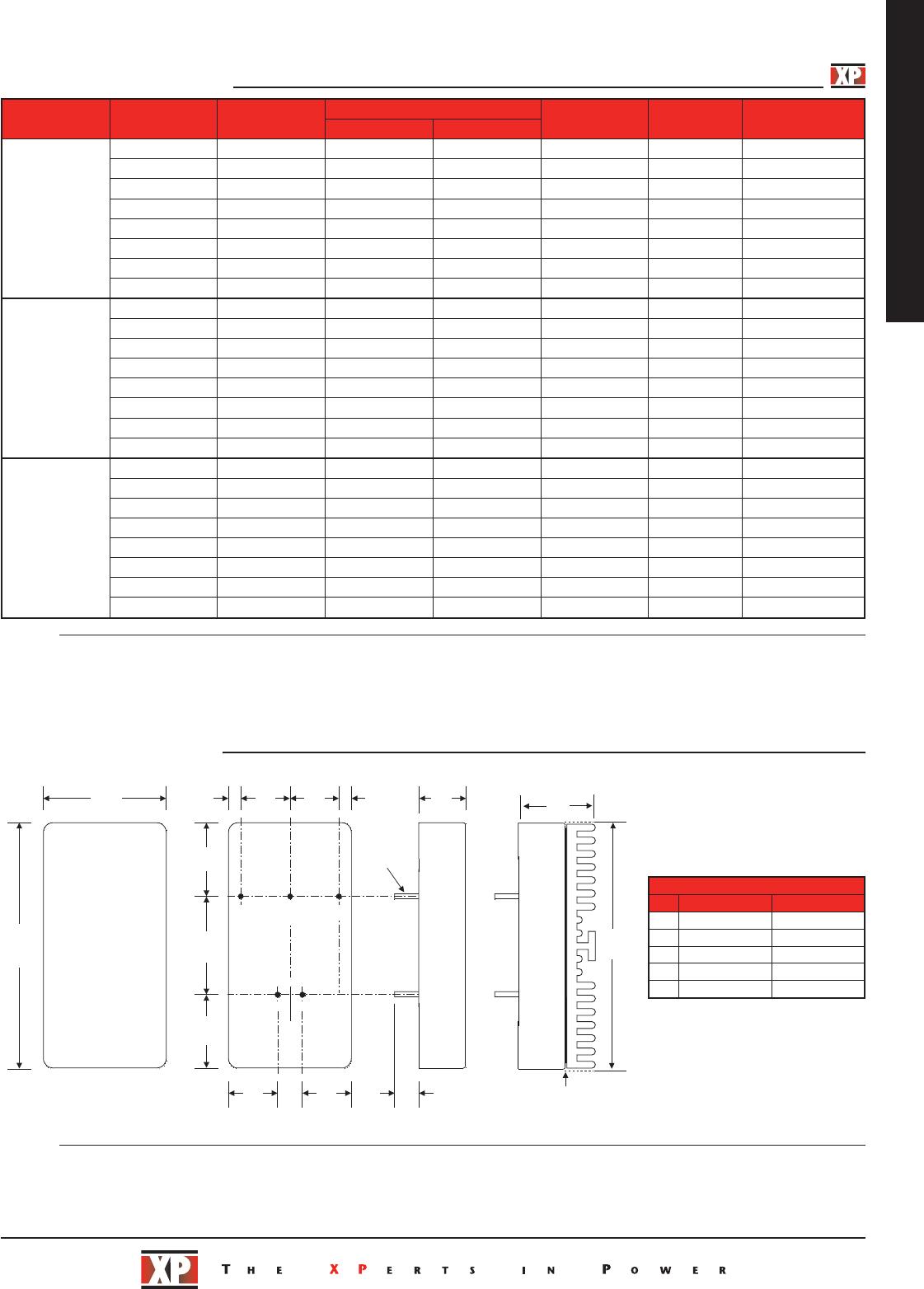
Models and Ratings
Notes
1. Measured at nominal input voltage.
2. When one output is set at 100% load and other varied between 25% and
100% load.
3. Measured with 20 MHz bandwidth and 1 µF ceramic capacitor across output rails.
4. For optional 3.5 kV isolation version, add suffix -H to part number
eg. JCK1524S12-H.
5. For heatsink option add ‘-HK’ to the end of the part number.
Notes
Mechanical Details
Input
Voltage
Output
Voltage
Output
Current
Input Current
(1)
Maximum
Capacitive Load
Efficiency Model Number
(4)
No Load Full Load
9-18 VDC
3.3 V 3.00 A 30 mA 1.03 A 3300 µF 82% JCK1512S3V3
5.0 V 3.00 A 30 mA 1.52 A 3300 µF 84% JCK1512S05
12.0 V 1.250 A 30 mA 1.45 A 1000 µF 88% JCK1512S12
15.0 V 1.000 A 30 mA 1.44 A 680 µF 89% JCK1512S15
±3.3 V ±1.500 A 30 mA 1.03 A ±1000 µF 82% JCK1512D03
±5.0 V ±1.500 A 30 mA 1.50 A ±1000 µF 85% JCK1512D05
±12.0 V ±0.625 A 30 mA 1.45 A ±470 µF 88% JCK1512D12
±15.0 V ±0.500 A 30 mA 1.45 A ±330 µF 88% JCK1512D15
18-36 VDC
3.3 V 3.000 A 25 mA 0.52 A 3300 µF 82% JCK1524S3V3
5.0 V 3.000 A 25 mA 0.75 A 3300 µF 85% JCK1524S05
12.0 V 1.250 A 25 mA 0.72 A 1000 µF 89% JCK1524S12
15.0 V 1.000 A 25 mA 0.72 A 680 µF 89% JCK1524S15
±3.3 V ±1.500 A 25 mA 0.52 A ±1000 µF 82% JCK1524D03
±5.0 V ±1.500 A 25 mA 0.75 A ±1000 µF 85% JCK1524D05
±12.0 V ±0.625 A 25 mA 0.72 A ±470 µF 88% JCK1524D12
±15.0 V ±0.500 A 25 mA 0.72 A ±330 µF 88% JCK1524D15
36-75 VDC
3.3 V 3.000 A 20 mA 0.26 A 3300 µF 82% JCK1548S3V3
5.0 V 3.000 A 20 mA 0.38 A 3300 µF 85% JCK1548S05
12.0 V 1.250 A 20 mA 0.36 A 1000 µF 89% JCK1548S12
15.0 V 1.000 A 20 mA 0.36 A 680 µF 89% JCK1548S15
±3.3 V ±1.500 A 20 mA 0.26 A ±1000 µF 82% JCK1548D03
±5.0 V ±1.500 A 20 mA 0.38 A ±1000 µF 85% JCK1548D05
±12.0 V ±0.625 A 20 mA 0.36 A ±470 µF 88% JCK1548D12
±15.0 V ±0.500 A 20 mA 0.36 A ±330 µF 88% JCK1548D15
PIN CONNECTIONS
Pin Single Dual
1 +Vin +Vin
2 -Vin -Vin
3 +Vout +Vout
4 No Pin Com
5 -Vout -Vout
1. All dimensions are in inches (mm).
2. Weight: 0.07 lbs (30 g)
3. Pin diameter: 0.04 ±0.002 (1.0 ±0.05)
4. Pin pitch tolerance: ±0.014 (±0.35)
5. Case tolerance: ±0.02 (±0.5)
DCDC
29-Oct-13
JCK15
A
pplication Notes
Derating Curve
Input Filter
12 µH
220 µF
+Vin
-Vin
+
-
50%
25%
7
5%
100%
-40 -20 0 20 40 60 80 100 120 140
85
7
0
75
Ambient Temperature (ºC)
Load (%)
w
ith heat-sink
without heat-sink

JCK1524D05

Mfr. #:
Manufacturer:
Description:
CONVERTER, DC/DC 15W, +/-5V
Lifecycle:
New from this manufacturer.
Delivery:
DHL FedEx Ups TNT EMS
Payment:
T/T Paypal Visa MoneyGram Western Union