LTC1061
4
1061fe
POWER SUPPLY VOLTAGE (±V)
0
I
SUPPLY
(mA)
8
1061 G09
6
3
0
2
4
6
10
9
15
21
18
24
13
5
7
9
27
30
12
T
A
= –55°C
T
A
= 25°C
T
A
= 125°C
CENTER FREQUENCY (kHz)
0
ERROR FROM IDEAL f
CLK
/f
O
(%)
32
1061 G08
1.0
0.5
0
8
16
24
40
1.5
0
1.0
0.5
1.5
412
20
28
36
Q = 10
T
A
= 25°C
f
CLK
/f
O
= 50/1
MODE 1,
MODE 3
V
S
= ±2.5V
V
S
= ±7.5V
V
S
= ±5V
MODE 3
2.0
2.5
MODE 3
MODE 1
MODE 1
V
S
= ±2.5V
MODE 1,3
V
S
= ±5V
MODE 1,3
V
S
= ±7.5V
MODE 1,3
Q = 10
T
A
= 25°C
f
CLK
/f
O
= 100/1
CENTER FREQUENCY (kHz)
0
DEVIATION FROM IDEAL Q (%)
32
1061 G07
20
10
0
8
16
24
30
0
20
10
30
412
20 28
Q=20
V
S
= ±2.5V V
S
= ±7.5V
20
10
10
V
S
= ±5V
Q=5
Q=20
Q=5
Q=1
10
Q=5
Q=1
CENTER FREQUENCY (kHz)
0
DEVIATION FROM IDEAL Q (%)
32
1061 G06
20
10
0
8
16
24
40
30
0
20
10
30
412
20
28
36
T
A
= 25°C
f
CLK
/f
O
= 50/1
20
5
Q=1
V
S
= ±2.5V
V
S
= ±7.5V
5
20
10
20
10
T
A
= 25°C
f
CLK
/f
O
= 50:1
V
S
= ±5V
10
2.5
Q=1
5
2.5
Q=1
CENTER FREQUENCY (kHz)
0
DEVIATION FROM IDEAL Q (%)
32
1061 G05
20
10
0
8
16
24
30
0
20
10
30
412
20 28
Q=20
V
S
= ±2.5V V
S
= ±7.5V
10
10
10
V
S
= ±5V
Q=5
Q<5
Q=20
Q=20 Q=5
CENTER FREQUENCY (kHz)
0
DEVIATION FROM IDEAL Q (%)
32
1061 G04
20
10
0
8
16
24
40
30
0
20
10
30
412
20
28
36
T
A
= 25°C
f
CLK
/f
O
= 50/1
20
50
10
Q<5
V
S
= ±2.5V
V
S
= ±7.5V
50
20
10
Q<5
50
20
10
Q<5
T
A
= 25°C
f
CLK
/f
O
= 50/1
V
S
= ±5V
IDEAL Q
0.1
0.2
DEVIATION OF f
CLK
/f
O
WITH RESPECT TO
Q = 10 MEASUREMENT (%)
0.1
0
0.1
1 10 100
1061 G03
.
0.3
0.4
0.5
V
S
= ±5V
T
A
= 25°C
PIN 7 AT 100:1
f
CLK
/f
O
= 500:1
R2/R4 = 1/5
(A)
(B)
R2/R4 = 1/2
f
CLK
/f
O
= 200:1
IDEAL Q
0.1
0.3
% DEVIATION (f
CLK
/f
O
)
0.2
0.1
0
0.1
1 10 100
1061 G02
.
0.4
0.5
0.6
V
S
= ±5V
T
A
= 25°C
f
CLK
= 500kHz
f
CLK
/f
O
=
100 (TEST POINT)
IDEAL Q
0.1
–1.6
% DEVIATION (f
CLK
/f
O
)
–1.2
0.8
0.4
0
1 10 100
1061 G01
2.0
2.4
0.4
V
S
= ±5V
T
A
= 25°C
f
CLK
= 250kHz
f
CLK
/f
O
=
50 (TEST POINT)
CCHARA TERIST
ICS
UW
AT
Y
P
I
CA
LPER
F
O
R
C
E
Mode 1, Mode 3 (f
CLK
/f
O
)
Deviation vs Q
Mode 1, Mode 3 (f
CLK
/f
O
)
Deviation vs Q
Mode 3: Deviation of (f
CLK
/f
O
)
with Respect to Q = 10
Measurement
Mode 1: (f
CLK
/f
O
) = 50:1
Mode 1: (f
CLK
/f
O
) = 100:1
Mode 3: (f
CLK
/f
O
) = 50:1
Mode 3: (f
CLK
/f
O
) = 100:1 f
CLK
/f
O
vs f
O
Power Supply Current vs
Supply Voltage
5
LTC1061
1061fe
DESCRIPTIO A D
U
PI
U
APPLICATIO
U
HI TS
UU
+
Σ
+
Σ
LEVEL
SHIFT
LEVEL
SHIFT
LEVEL
SHIFT
CLOCK
GENERATOR
CLOCK
GENERATOR
CLOCK
GENERATOR
CLK
(8)
LEVEL SHIFT
(9)
TO FILTER A
TO FILTER B
TO FILTER C
+
+
+
+
+
50/100/
HOLD
(7)
AGND
(6)
V
+
(10)
V
(15)
HP
C
(12)
S1
B
(16)
BP
C
(13)
LP
C
(14)
S1
A
(5)
NB
(18)
BP
B
(19)
LP
B
(20)
NA
(3)
BP
A
(2)
LP
A
(1)
INV
A
(4)
INV
B
(17)
INV
C
(11)
1061 BD
+
+
+
+
frequencies below 500kHz the clock “on” time can be as
low as 300ns. The maximum clock frequency for ±5V
supplies and above is 2.4MHz.
S1
A
, S1
B
(Pins 5, 16)
These are voltage input pins. If used, they should be driven
with a source impedance below 5k. when they are not
used, they should be tied to the analog ground Pin 6.
AGND (Pin 6)
When the LTC1061 operates with dual supplies, Pin 6
should be tied to system ground. When the LTC1061
operates with a single positive supply, the analog ground
pin should be tied to 1/2 supply, Figure 1. The positive
input of all the internal op amps, as well as the common
reference of all the internal switches, are internally tied to
the analog ground pin. Because of this, a “clean” ground
is recommended.
Power Supplies (Pins 10, 15)
They should be bypassed with 0.1µF disc ceramic. Low
noise, nonswitching, power supplies are recommended.
The device operates with a single 5V supply, Figure 1, and
with dual supplies. The absolute maximum operating
power supply voltage is ±9V.
Clock and Level shift (Pins 8, 9)
When the LTC1061 operates with symmetrical dual sup-
plies the level shift Pin 9 should be tied to analog ground.
For single 5V supply operation, the level shift pin should be
tied to Pin 15 which will be the system ground. The typical
logic threshold levels of the clock pin are as follows: 1.65V
above the level shift pin for ±5V supply operation, 1.75V
for ±7.5V and above, and 1.4V for single 5V supply
operation. The logic threshold levels vary ±100mV over
the full military temperature range. The recommended
duty cycle of the input clock is 50% although for clock
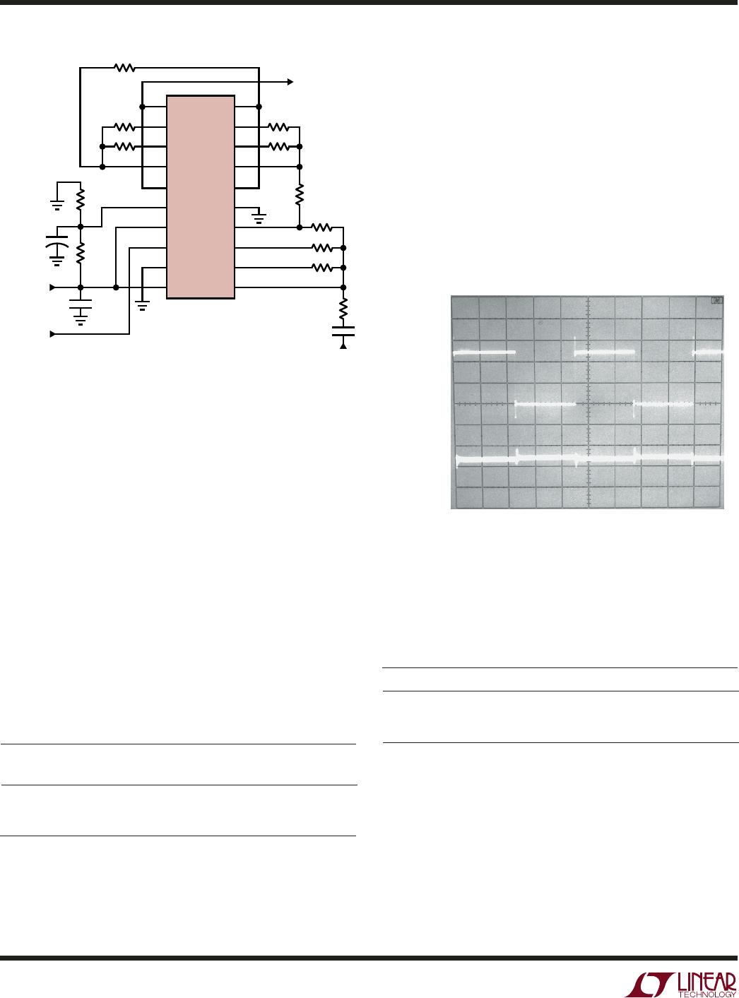
BLOCK DIAGRA
W
LTC1061
6
1061fe
Figure 1. The 6th Order LP Butterworth Filter of Figure 5
Operating with a Single 5V Supply
20
19
18
17
16
15
14
13
12
11
1
2
3
4
5
6
7
8
9
10
R3
V
OUT
R1
V
IN
0.1µF
1061 F01
LTC1061
+
R2
R1
R3
R2
R4
R1
R3
R2
T
2
L CLOCK
IN
f
CLK
< 1MHz
1µF
5V
2.49k
2.49k
C
IN
Clock Feedthrough
This is defined as the amplitude of the clock frequency
appearing at the output pins of the device, Figure 2. Clock
feedthrough is measured with all three sides of the LTC1061
connected as filters. The clock feedthrough mainly de-
pends on the magnitude of the power supplies and it is
independent from the input clock levels, clock frequency
and modes of operation.
The Table 2 illustrates the typical clock feedthrough num-
bers for various power supplies.
50/100/Hold (Pin 7)
By tying Pin 7 to V
+
, the filter operates with a clock-to-
center frequency internally set at 50:1. When Pin 7 is at
mid-supplies, the filter operates with a 100:1 clock-to-
center frequency ratio. Table 1 shows the allowable varia-
tion of the potential at Pin 7 when the 100:1 mode is
sought.
When Pin 7 is shorted to the negative supply pin, the filter
operation is stopped and the bandpass and lowpass
output act as a sample-and-hold circuit holding the last
sample of the input voltage. The hold step is around 2mV
and the droop rate is 150µV/sec.
Table 1
TOTAL POWER SUPPLY VOLTAGE RANGE OF PIN 7
(V) FOR 100:1 OPERATION (V)
5 2.5 ± 0.5
10 5 ±1
15 7.5 ±1.5
Figure 2. Typical Clock Feedthrogh of the LTC1061 Operating
with ±5V Supplies. Top Trace is the Input Clock Swinging 0V to
5V and Bottom Trace is One of the Lowpass Outputs with Zero or
DC Input Signals.
A = 2V/DIV
B = 10mV/DIV
HORIZONTAL = 10µs/DIV
POWER SUPPLY (V) CLOCK FEEDTHROUGH (V
RMS
)
±2.5 0.2
±5 0.4
±8 0.8
Table 2
Definition of Filter Functions
Refer to LTC1060 data sheet.
1061 F02
DESCRIPTIO A D
U
PI
U
APPLICATIO
U
HI TS
UU

LTC1061ACN#PBF

Mfr. #:
Manufacturer:
Analog Devices Inc.
Description:
Active Filter Triple Switched Capacitor Filter
Lifecycle:
New from this manufacturer.
Delivery:
DHL FedEx Ups TNT EMS
Payment:
T/T Paypal Visa MoneyGram Western Union