NRVB0540T3G

Semiconductor Components Industries, LLC, 2012
January, 2012 Rev. 7
1 Publication Order Number:
MBR0540T1/D
MBR0540T1G,
NRVB0540T1G,
MBR0540T3G,
NRVB0540T3G
Surface Mount
Schottky Power Rectifier
SOD123 Power Surface Mount Package
The Schottky Power Rectifier employs the Schottky Barrier
principle with a barrier metal that produces optimal forward voltage
dropreverse current tradeoff. Ideally suited for low voltage, high
frequency rectification, or as a free wheeling and polarity protection
diodes in surface mount applications where compact size and weight
are critical to the system. This package provides an alternative to the
leadless 34 MELF style package.
Features
Guardring for Stress Protection
Very Low Forward Voltage
Epoxy Meets UL 94 V0 @ 0.125 in
Package Designed for Optimal Automated Board Assembly
AECQ101 Qualified and PPAP Capable
NRVB Prefix for Automotive and Other Applications Requiring
Unique Site and Control Change Requirements
All Packages are PbFree*
Mechanical Characteristics
Device Marking: B4
Polarity Designator: Cathode Band
Weight: 11.7 mg (approximately)
Case: Epoxy Molded
Finish: All External Surfaces Corrosion Resistant and Terminal
Leads are Readily Solderable
Lead and Mounting Surface Temperature for Soldering Purposes:
260C max. for 10 Seconds
ESD Rating:
Human Body Model = 3B
Machine Model = C
*For additional information on our PbFree strategy and soldering details, please
download the ON Semiconductor Soldering and Mounting Techniques
Reference Manual, SOLDERRM/D.
B4 = Device Code
M = Date Code
G = PbFree Package
http://onsemi.com
SCHOTTKY BARRIER
RECTIFIER
0.5 AMPERES, 40 VOLTS
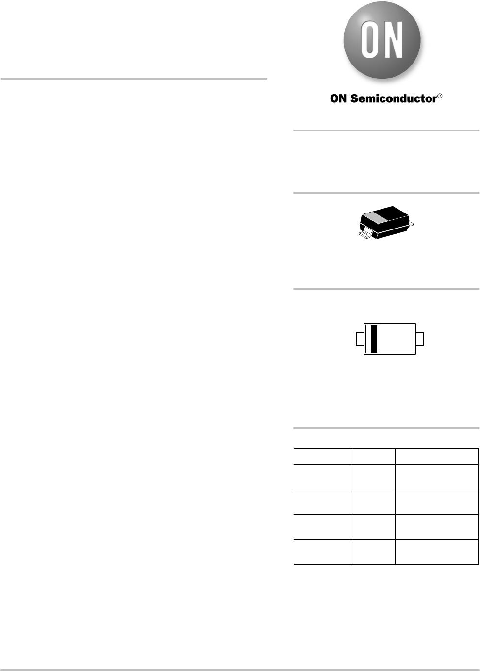
SOD123
CASE 425
STYLE 1
MARKING DIAGRAM
Device Package Shipping
ORDERING INFORMATION
MBR0540T1G SOD123
(PbFree)
3,000/Tape & Reel
(8 mm Tape, 7” Real)
MBR0540T3G SOD123
(PbFree)
10,000/Tape & Reel
(8 mm Tape, 13” Real)
For information on tape and reel specifications,
including part orientation and tape sizes, please
refer to our Tape and Reel Packaging Specifications
Brochure, BRD8011/D.
(Note: Microdot may be in either location)
NRVB0540T1G SOD123
(PbFree)
3,000/Tape & Reel
(8 mm Tape, 7” Real)
NRVB0540T3G SOD123
(PbFree)
10,000/Tape & Reel
(8 mm Tape, 13” Real)
B4MG
G
1
MBR0540T1G, NRVB0540T1G, MBR0540T3G, NRVB0540T3G
http://onsemi.com
2
MAXIMUM RATINGS
Rating Symbol Value Unit
Peak Repetitive Reverse Voltage
Working Peak Reverse Voltage
DC Blocking Voltage
V
RRM
V
RWM
V
R
40 V
Average Rectified Forward Current
(At Rated V
R
, T
C
= 115C)
I
O
0.5
A
Peak Repetitive Forward Current
(At Rated V
R
, Square Wave, 20 kHz, T
C
= 115C)
I
FRM
1.0
A
NonRepetitive Peak Surge Current
(Surge Applied at Rated Load Conditions Halfwave, Single Phase, 60 Hz)
I
FSM
5.5
A
Storage/Operating Case Temperature Range T
stg
, T
C
55 to +150 C
Operating Junction Temperature T
J
55 to +150 C
Voltage Rate of Change
(Rated V
R
, T
J
= 25C)
dv/dt
1000
V/ms
Stresses exceeding Maximum Ratings may damage the device. Maximum Ratings are stress ratings only. Functional operation above the
Recommended Operating Conditions is not implied. Extended exposure to stresses above the Recommended Operating Conditions may affect
device reliability.
THERMAL CHARACTERISTICS
Characteristic Symbol Value Unit
Thermal Resistance JunctiontoLead (Note 1)
Thermal Resistance JunctiontoAmbient (Note 2)
R
tjl
R
tja
118
206
C/W
1. Mounted with minimum recommended pad size, PC Board FR4.
2. 1 inch square pad size (1 X 0.5 inch for each lead) on FR4 board.
ELECTRICAL CHARACTERISTICS
Characteristic Symbol Value Unit
Maximum Instantaneous Forward Voltage (Note 3)
v
F
T
J
= 25C T
J
= 100C
V
(i
F
= 0.5 A)
(i
F
= 1 A)
0.51
0.62
0.46
0.61
Maximum Instantaneous Reverse Current (Note 3)
I
R
T
J
= 25C T
J
= 100C mA
(V
R
= 40 V)
(V
R
= 20 V)
20
10
13,000
5,000
3. Pulse Test: Pulse Width 250 ms, Duty Cycle 2.0%.
0.2
10
1.0
0.1
0.6 1.20.4 0.8 1.0
Figure 1. Typical Forward Voltage Figure 2. Maximum Forward Voltage
0.2
v
F
, INSTANTANEOUS FORWARD VOLTAGE (VOLTS)
10
1.0
V
F
, MAXIMUM INSTANTANEOUS FORWARD VOLTAGE (VOLTS)
i
F
, INSTANTANEOUS FORWARD CURRENT (AMPS)
0.1
0.6 1.20.4 0.8
I
F
, INSTANTANEOUS FORWARD CURRENT (AMPS)
T
J
= 125C
T
J
= 100C
T
J
= -40C
T
J
= 25C
T
J
= 125C
T
J
= 100C
T
J
= 25C
100
1.0
25C
MBR0540T1G, NRVB0540T1G, MBR0540T3G, NRVB0540T3G
http://onsemi.com
3
Figure 3. Typical Reverse Current Figure 4. Maximum Reverse Current
400
V
R
, REVERSE VOLTAGE (VOLTS)
100E-3
1.0E-3
100E-6
10E-6
1.0E-6
100E-9
V
R
, REVERSE VOLTAGE (VOLTS)
I
10 20 30
, REVERSE CURRENT (AMPS)
R
400
I
10 20 30
, MAXIMUM REVERSE CURRENT (AMPS)
R
T
J
= 125C
T
J
= 100C
T
J
= 25C
T
J
= 100C
T
J
= 25C
10E-3
100E-3
1.0E-3
100E-6
10E-6
1.0E-6
100E-9
10E-3
Figure 5. Current Derating Figure 6. Forward Power Dissipation
20 600
T
L
, LEAD TEMPERATURE (C)
0.8
0.4
0.3
0.2
0.1
0
I
O
, AVERAGE FORWARD CURRENT (AMPS)
0.10
0.45
0.40
0.35
0.15
0.05
0
0.440
, AVERAGE FORWARD CURRENT (AMPS)I
O
80 120100
0.5
0.2 0.3 0.5 0.8
0.10
P
FO
, AVERAGE POWER DISSIPATION (WATTS)
140
0.6
SQUARE WAVE
dc
I
pk
/I
o
= p
I
pk
/I
o
= 5
I
pk
/I
o
= 10
I
pk
/I
o
= 20
I
pk
/I
o
= 20
I
pk
/I
o
= 10
I
pk
/I
o
= 5
I
pk
/I
o
= p
SQUARE WAVE
dc
0.7
0.30
0.20
0.25
0.6 0.7
FREQ = 20 kHz
Figure 7. Capacitance Figure 8. Typical Operating Temperature Derating*
300
V
R
, REVERSE VOLTAGE (VOLTS)
100
10
V
R
, DC REVERSE VOLTAGE (VOLTS)
25 400
118
114
112
110
C, CAPACITANCE (pF)
T
155.0 10 20 25 35 40 30 355.0 10 2015
116
120
126
, DERATED OPERATING TEMPERATURE ( C)
J
* Reverse power dissipation and the possibility of thermal runaway must be considered when operating this device under any
reverse voltage conditions. Calculations of T
J
therefore must include forward and reverse power effects. The allowable operating
T
J
may be calculated from the equation: T
J
= T
Jmax
r(t)(Pf + Pr) where
r(t) = thermal impedance under given conditions,
Pf = forward power dissipation, and
Pr = reverse power dissipation
This graph displays the derated allowable T
J
due to reverse bias under DC conditions only and is calculated as
T
J
= T
Jmax
r(t)Pr, where r(t) = Rthja. For other power applications further calculations must be performed.
R
tja
= 118C/W
180C/W
149C/W
206C/W
228C/W
T
J
= 25C
122
124

NRVB0540T3G

Mfr. #:
Manufacturer:
ON Semiconductor
Description:
Schottky Diodes & Rectifiers REC SCHKY 40V TR
Lifecycle:
New from this manufacturer.
Delivery:
DHL FedEx Ups TNT EMS
Payment:
T/T Paypal Visa MoneyGram Western Union

Products related to this Datasheet