VO0601-X001T

VO0600T, VO0601T, VO0611T, VO0630T, VO0631T, VO0661T
www.vishay.com
Vishay Semiconductors
Rev. 2.0, 25-Oct-12
7
Document Number: 84607
For technical questions, contact: optocoupleranswers@vishay.com
THIS DOCUMENT IS SUBJECT TO CHANGE WITHOUT NOTICE. THE PRODUCTS DESCRIBED HEREIN AND THIS DOCUMENT
ARE SUBJECT TO SPECIFIC DISCLAIMERS, SET FORTH AT www.vishay.com/doc?91000
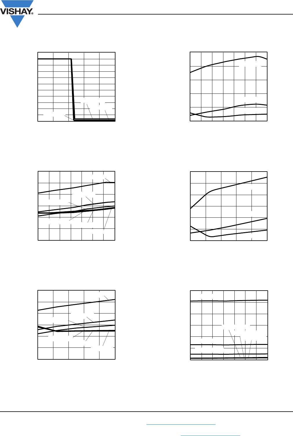
Fig. 10 - High Level Supply Current vs. Ambient Temperature
Fig. 11 - Input Threshold On Current vs. Ambient Temperature
Fig. 12 - Input Threshold Off Current vs. Ambient Temperature
Fig. 13 - Low Level Output Voltage vs. Ambient Temperature
Fig. 14 - Low Level Output Current vs. Ambient Temperature
Fig. 15 - High Level Output Current vs. Ambient Temperature
2.8
2.9
3.0
3.1
3.2
3.3
3.4
3.5
- 40 - 20 0 20 40 60 80 100
I
CCH
- High Level Supply Current (mA)
T
amb
- Ambient Temperature (°C)
17615
V
CC
= 7 V
I
F
= 0.25 mA
V
CC
= 5 V
I
F
= 0.25 mA
2.0
2.1
2.2
2.3
2.4
2.5
2.6
- 40 - 20 0 20 40 60 80 100
I
TH
- Input Threshold Off Current (µA)
T
amb
- Ambient Temperature (°C)
17617
R
L
= 350 Ω
R
L
= 4 kΩ
R
L
= 1 kΩ
0.00
0.05
0.10
0.15
0.20
0.25
0.30
- 40 - 20 0 20 40 60 80 100
V
OL
- Low Level Output Voltage (V)
T
amb
- Ambient Temperature (°C)
17618
I
L
= 6 mA
I
L
= 10 mA
I
L
= 13 mA
I
L
= 16 mA
V
CC
= 5.5 V
I
F
= 5 mA
0
10
20
30
40
50
60
- 40 - 20 0 20 40 60 80 100
I
OL
- Low Level Output Current (mA)
T
amb
- Ambient Temperature (°C)
17619
I
F
= 5 mA
I
F
= 10 mA
0
5
10
15
20
25
30
35
40
45
50
- 40 - 20 0 20 40 60 80 100
I
OH
- High Level Output Current (nA)
T
amb
- Ambient Temperature (°C)
17620
VO0600T, VO0601T, VO0611T, VO0630T, VO0631T, VO0661T
www.vishay.com
Vishay Semiconductors
Rev. 2.0, 25-Oct-12
8
Document Number: 84607
For technical questions, contact: optocoupleranswers@vishay.com
THIS DOCUMENT IS SUBJECT TO CHANGE WITHOUT NOTICE. THE PRODUCTS DESCRIBED HEREIN AND THIS DOCUMENT
ARE SUBJECT TO SPECIFIC DISCLAIMERS, SET FORTH AT www.vishay.com/doc?91000
Fig. 16 - Output Voltage vs. Forward Input Current
Fig. 17 - Propagation Delay vs. Ambient Temperature
Fig. 18 - Propagation Delay vs. Forward Current
Fig. 19 - Pulse Width Distortion vs. Ambient Temperature
Fig. 20 - Pulse Width Distortion vs. Forward Current
Fig. 21 - Rise and Fall Time vs. Ambient Temperature
0.0
0.5
1.0
1.5
2.0
2.5
3.0
3.5
4.0
4.5
5.0
5.5
0
V
o
- Output Voltage (V)
I
F
- Forward Input Current (mA)
17621
R
L
= 350 Ω
5
43
21
R
L
= 1 kΩ
R
L
= 4 kΩ
0
20
40
60
80
100
120
- 40 - 20 0 20 40 60 80 100
T
amb
- Ambient Temperature (°C)
17622
t
P
- Propagation Delay Time (ns)
t
PLH
, 4 kΩ
t
PLH
, 1 kΩ
t
PLH
, 350 Ω
t
PHL
, 350 Ω
t
PHL
, 1 kΩ
t
PHL
, 4 kΩ
0
20
40
60
80
100
120
5111315
I
F
- Forward Current (mA)
17623
t
P
- Propagation Delay Time (ns)
t
PLH
, 4 kΩ
97
t
PLH
, 1 kΩ
t
PLH
, 350 Ω
t
PHL
, 350 Ω
t
PHL
, 1 kΩ
t
PHL
, 4 kΩ
0
10
20
30
40
50
- 40 - 20 0 20 40 60 80 100
T
amb
- Ambient Temperature (°C)
17624
PWD - Pulse Width Distortion (ns)
R
L
= 4 kΩ
R
L
= 1 kΩ
R
L
= 350 Ω
0
10
20
30
40
50
60
5111315
I
F
- Forward Current (mA)
17625
PWD - Pulse Width Distortion (ns)
R
L
= 4 kΩ
9
7
R
L
= 1 kΩ
R
L
= 350 Ω
0
50
100
150
200
250
300
- 40 - 20 0 20 40 60 80 100
T
amb
- Ambient Temperature (°C)
17626
t
r, f
- Rise and Fall Time (ns)
t
r
, R
L
= 4 kΩ
t
f
, R
L
= 350 Ω
t
f
, R
L
= 1 kΩ
t
f
, R
L
= 4 kΩ
t
r
, R
L
= 1 kΩ
t
r
, R
L
= 350 Ω
VO0600T, VO0601T, VO0611T, VO0630T, VO0631T, VO0661T
www.vishay.com
Vishay Semiconductors
Rev. 2.0, 25-Oct-12
9
Document Number: 84607
For technical questions, contact: optocoupleranswers@vishay.com
THIS DOCUMENT IS SUBJECT TO CHANGE WITHOUT NOTICE. THE PRODUCTS DESCRIBED HEREIN AND THIS DOCUMENT
ARE SUBJECT TO SPECIFIC DISCLAIMERS, SET FORTH AT www.vishay.com/doc?91000
Fig. 22 - Rise and Fall Time vs. Forward Current Fig. 23 - Enable Propagation Delay vs. Ambient Temperature
PACKAGE DIMENSIONS in millimeters
PACKAGE MARKING (example)
Notes
The VDE Logo is only marked on option1 parts.
Tape and reel suffix (T) is not part of the package marking.
ESD CAUTION
This is an ESD (electro static discharge) sensitive device. Electrostatic charges accumulate on the human body and test
equipment and can discharge without detection. Therefore, proper ESD precautions are recommended to avoid performance
degradation or loss of functionality. ESD withstand voltage of this device is up to 1500 V acc. to JESD22-A114-B.
0
50
100
150
200
250
300
5111315
I
F
- Forward Current (mA)
17627
t
r, f
- Rise and Fall Time (ns)
t
r
, R
L
= 4 kΩ
97
t
r
, R
L
= 1 kΩ
t
r
, R
L
= 350 Ω
t
f
, R
L
= 350 Ω
t
f
, R
L
= 1 kΩ
t
f
, R
L
= 4 kΩ
0
10
20
30
40
50
60
- 40 - 20 0 20 40 60 80 100
T
amb
- Ambient Temperature (°C)
17628
t
E
- Enable Propagation Delay (ns)
t
ELH
= 4 kΩ
t
ELH
= 350 Ω
t
EHL
= 350 Ω
t
EHL
= 4 kΩ
t
ELH
= 1 kΩ
t
EHL
= 1 kΩ
0.91
0.36
4.32
1.14
6.6
R 0.13
1.27
i178020-3
ISO methode A
40°
6.10
1.27 typ.
0.41
0.10
0.20
Lead coplanarity
± 0.001 max.
0.20
3.05 ± 0.05
C
L
R 0.25 max.
1.02
5° max.
Pin one ID
3.91 ± 0.05
0.38 ± 0.05
4.88 ± 0.05
0.51 ± 0.10
2 plcs.
1.49 ± 0.05
3.18 ± 0.05
0601X1
V YWW Y68

VO0601-X001T

Mfr. #:
Manufacturer:
Vishay Semiconductors
Description:
Triac & SCR Output Optocouplers H. Speed Optocplr 10MBd 5kV/us CMR VDE
Lifecycle:
New from this manufacturer.
Delivery:
DHL FedEx Ups TNT EMS
Payment:
T/T Paypal Visa MoneyGram Western Union