MAX749
Digitally Adjustable LCD Bias Supply
4 ______________________________________________________________________________________
PIN NAME FUNCTION
1 V+
+2V to +6V Input Voltage to power the MAX749 and external circuitry. When using an external
P-channel MOSFET, V+ must exceed the MOSFET’s gate threshold voltage.
2 ADJ
Logic Input. When CTRL is high, a rising edge on ADJ increments an internal counter. When CTRL is
low, the counter is reset to mid-scale when ADJ is high. When ADJ is low, the counter does not
change (regardless of activity on CTRL) as long as V+ is applied.
3 CTRL
Logic Input. When CTRL and ADJ are low, the MAX749 is shut down, but the counter is not reset.
When CTRL is low, the counter is reset to mid-scale when ADJ is high. The device is always on when
CTRL is high.
4 FB
Feedback Input for output full-scale voltage selection. -V
OUT
(MAX)
= (R
FB
) x (20µA) where R
FB
is
connected from FB to -V
OUT
. The device is in regulation when V
FB
= 0V.
5 GND Ground
6 DLOW
Output Driver Low. Connect to DHI when using an external P-channel MOSFET. When using an
external PNP transistor, connect a resistor R
BASE
from DLOW to the base of the PNP to set the maxi-
mum base-drive current.
7 DHI
Output Driver High. Connect to the gate of the external P-channel transistor, or to the base of the
external PNP transistor.
8 CS
Current-Sense Input. The external transistor is turned off when current through the sense resistor,
R
SENSE
, brings CS below V+ by 140mV (typ).
OUTPUT
VOLTAGE
LOAD
CURRENT
100mV
AC
/div
10mA/div
0mA
LOAD-TRANSIENT RESPONSE
V
OUT
= -15V
TRANSISTOR = ZTX750
50µs/div
V
OUT
= -15V
TRANSISTOR = ZTX750
OUTPUT
VOLTAGE
INPUT
VOLTAGE
100mV
AC
/div
1 V/div
0V
LINE-TRANSIENT RESPONSE
V
OUT
= -15V
I
LOAD
= 5mA
TRANSISTOR = ZTX750
50ms/div
____________________________Typical Operating Characteristics (continued)
(T
A
= +25°C, L = 47µH, unless otherwise noted.)
______________________________________________________________Pin Description
_______________Detailed Description
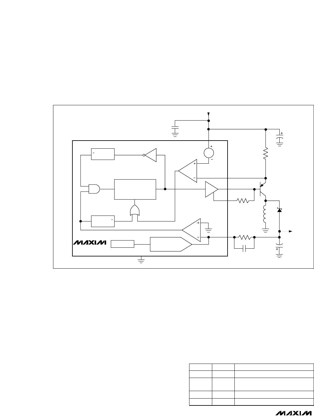
The MAX749 is a negative-output inverting power con-
troller that can drive an external PNP transistor or P-
channel MOSFET. An external resistor and an internal
DAC control the output voltage (Figure 1).
The MAX749 is designed to operate from 2V to 6V inputs,
ideal for operation from low-voltage batteries. In systems
with higher-voltage batteries, such as notebook comput-
ers, the MAX749 may also be operated from the regulat-
ed +5V supply. A high-efficiency +5V regulator, such as
the MAX782, is an ideal source for the MAX749. In this
example, the MAX749 efficiency (80%) is compounded
with the MAX782 efficiency (95%): 80% x 95% = 76%,
which is still high.
Operating Principle
The MAX749 and the external components shown in the
Typical Operating Circuit
form a flyback converter.
When the external transistor is on, current flows through
the current-sense resistor, the transistor, and the coil.
Energy is stored in the core of the coil during this phase,
and the diode does not conduct. When the transistor
turns off, current flows from the output through the diode
and the coil, driving the output negative. Feedback con-
trol adjusts the external transistor’s timing to provide a
regulated negative output voltage.
The MAX749’s unique control scheme combines the
ultra-low supply current of pulse-skipping, pulse-fre-
quency modulation (PFM) converters with the high full-
load efficiency characteristic of pulse-width modulation
(PWM) converters. This control scheme allows the
device to achieve high efficiency over a wide range of
loads. The current-sense function and high operating
frequency allow the use of tiny external components.
Switching control is accomplished through the combi-
nation of a current limit in the switch plus on- and off-
time limits (Figure 2).
Once turned on, the transistor stays on until either:
- the maximum on-time one-shot turns it off
(8µs later), or
- the switch current reaches its limit (as determined
by the current-sense resistor and the current
comparator).
MAX749
Digitally Adjustable LCD Bias Supply
_______________________________________________________________________________________ 5
L1
47µH
DLOW
SWITCH-
MODE
POWER
SUPPLY
6-BIT
CURRENT-OUTPUT
DAC
REF
LOGIC
BIAS
POWER-ON
RESET
6-BIT
COUNTER
MAX749
V
OUT
(NEGATIVE)
CTRL
ADJ
RESET
INCREMENT
ON/OFF
+2V TO +6V
INPUT
22µF
6.2V
6.66µA TO 20µA
CS
DHI
FB
GND
R
SENSE
Q1
ZTX750
D1
1N5819
R
BASE
470
22µF
30V
C
COMP
R
FB
V+
0.1µF
Figure 1. Block Diagram, Showing External Circuitry Using a PNP Transistor
MAX749
Once turned off, a one-shot holds the switch off for a
minimum of 1µs, and the switch either stays off (if the
output is in regulation), or turns on again (if the output
is out of regulation).
With light loads, the transistor switches for one or more
cycles and then turns off, much like a traditional PFM
converter. With heavy loads, the transistor stays on until
the switch current reaches the current limit; it then
shuts off for 1µs, and immediately turns on again until
the next time the switch current reaches its limit. This
cycle repeats until the output is in regulation.
Output Voltage Control
The output voltage is set using a single external resistor
and the internal current-output DAC (Figure 1). The full-
scale output voltage is set by selecting the feedback
resistor, R
FB
. The output voltage is controlled from 33%
to 100% of the full-scale output by an internal 64-step
DAC/counter.
On power-up or after a reset, the counter sets the DAC
output to mid-range. Each rising edge of ADJ incre-
ments the DAC output. When incremented beyond full
scale, the counter rolls over and sets the DAC to the
minimum value. In this way, a single pulse applied to
ADJ increases the DAC set point by one step, and 63
pulses decrease the set point by one step.
Table 1 is the logic table for the CTRL and ADJ inputs,
which control the internal DAC and counter. Figures 3-7
show various timing specifications and different ways of
incrementing and resetting the DAC, and of placing it in
the low-power standby mode. As long as the timing
specifications for ADJ and CTRL are observed, any
sequence of operations can be implemented.
Table 1. Input Truth Table
Digitally Adjustable LCD Bias Supply
6 ______________________________________________________________________________________
L1
47µH
DLOW
6-BIT
CURRENT-OUTPUT
DAC
REF
MAXIMUM
ON-TIME
ONE-SHOT
MAX749
V
OUT
(NEGATIVE)
22µF
0.1µF
V+
DHI
FB
GND
R
SENSE
Q1
ZTX750
D1
1N5819
R
BASE
470
22µF
30V
C
COMP
R
FB
TRIG
MINIMUM
OFF-TIME
ONE-SHOT
TRIG
Q
Q
Q
S
R
FLIP-FLOP
VOLTAGE
COMPARATOR
140mV
+2V TO +6V 
INPUT
CURRENT
COMPARATOR
Figure 2. Switch-Mode Power-Supply Section Block Diagram
ADJ CTRL RESULT
Low Low Shut down
High Low
Reset counter to mid-range. The
device is not shut down.
X High On
High Increment the counter

MAX749CSA+T

Mfr. #:
Manufacturer:
Maxim Integrated
Description:
Display Drivers & Controllers Digitally Adjustable LCD Bias Supply
Lifecycle:
New from this manufacturer.
Delivery:
DHL FedEx Ups TNT EMS
Payment:
T/T Paypal Visa MoneyGram Western Union