MARCH 28, 2017 7 1.8V TO 3.3V LVCMOS HIGH PERFORMANCE CLOCK BUFFER FAMILY
5PB11xx DATASHEET
Notes:
1. With rail to rail input clock
2. Between any 2 outputs with equal loading.
3. Duty cycle on outputs will match incoming clock duty cycle. Consult IDT for tight duty cycle clock generators.
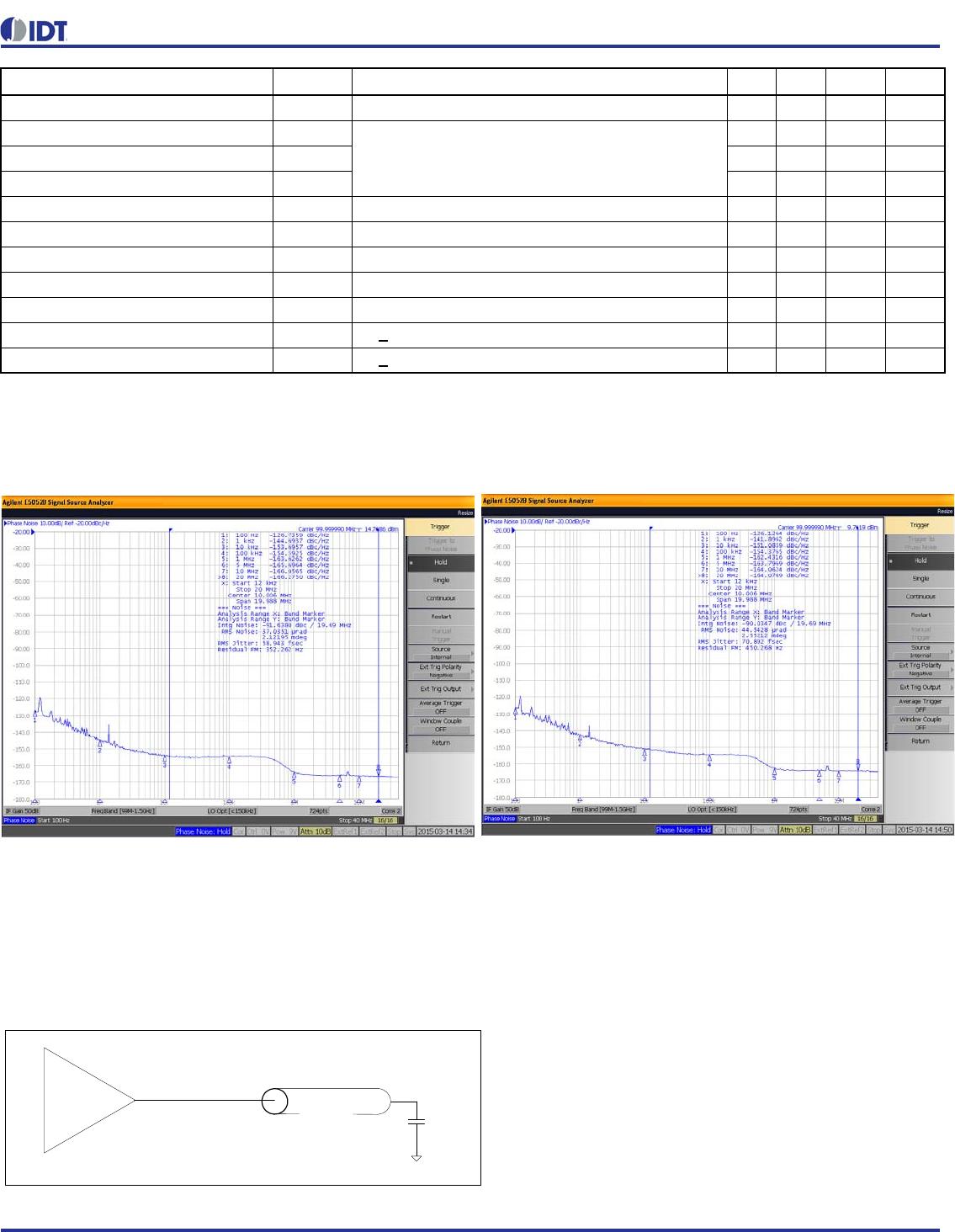
Phase Noise Plots
The phase noise plots above show the low additive jitter of the 5PB11xx high-performance buffer. With an integration range of
12kHz to 20MHz, the reference input has about 58.9fs of RMS phase jitter while the output of 5PB11xx has about 70.9fs of RMS
phase jitter. This results in a low additive phase jitter of only 39fs.
Test Load and Circuit
Start-up Time t
START-UP
Part start-up time for valid outputs after VDD ramp-up 3 ms
Propagation Delay (5PB1102/04)
Note 1
1.7 2 2.4 ns
Propagation Delay (5PB1106/08) 1.7 2 2.7 ns
Propagation Delay (5PB1110) 1.7 2 2.5 ns
Buffer Additive Phase Jitter, RMS 156.25MHz, Integration Range: 12kHz-20MHz 0.05 ps
Output to Output Skew (5PB1102/04) Rising edges at VDD/2, Note 2 35 50 ps
Output to Output Skew (5PB1106) Rising edges at VDD/2, Note 2 35 58 ps
Output to Output Skew (5PB1108/10) Rising edges at VDD/2, Note 2 45 65 ps
Device to Device Skew Rising edges at VDD/2 200 ps
Output Enable Time t
EN
C
L
< 5pF 3 cycles
Output Disable Time t
DIS
C
L
< 5pF 3 cycles
Parameter Symbol Conditions Min. Typ. Max. Units
Figure 1. 5PB11xx Reference Phase Noise 58.9fs
(12kHz to 20MHz)
Figure 2. 5PB11xx Output Phase Noise 70.9fs
(12kHz to 20MHz)
5
i
n
c
h
e
s
CL = 5pF
50ohms
1.8V TO 3.3V LVCMOS HIGH PERFORMANCE CLOCK BUFFER FAMILY 8 MARCH 28, 2017
5PB11xx DATASHEET
Marking Diagrams (industrial temperature range)
Notes:
1. “AA” denotes the last two digits of the part number for 8-pin TSSOP and DFN (e.g. 02, 04).
2. “
**” is the lot sequence.
3. “XXX” denotes the last three characters of the Asm lot (20-pin QFN only).
4. “YYWW”, “YWW”, “YW”, or “Y” is the last digit(s) of the year and week that the part was assembled.
5. “$” denotes the mark code.
6. “G” after the two-letter package code denotes RoHS compliant package.
7. “I” denotes industrial temperature range device.
8. Bottom marking: LOT and COO (TSSOP only).
11AA
YW**
8-pin DFN
XXX
YWW$
110I
20-pin QFN
1106
Y**
16-pin QFN
1108
Y**
16-pin QFN
IDT5PB11
10PGGI
YYWW$
20-pin TSSOP
YWW$
B11AAI
8-pin TSSOP
IDT5PB11
06PGGI
YYWW$
14-pin TSSOP
IDT5PB11
08PGGI
YYWW$
16-pin TSSOP
MARCH 28, 2017 9 1.8V TO 3.3V LVCMOS HIGH PERFORMANCE CLOCK BUFFER FAMILY
5PB11xx DATASHEET
Marking Diagrams (extended temperature range)
Notes:
1. “AA” denotes the last two digits of the part number for 8-pin TSSOP and DFN (e.g. 02, 04).
2. “
**” is the lot sequence.
3. “XXX” denotes the last three characters of the Asm lot (20-pin QFN only).
4. “YYWW”, “YWW”, “YW”, or “Y” is the last digit(s) of the year and week that the part was assembled.
5. “$” denotes the mark code.
6. “G” after the two-letter package code denotes RoHS compliant package.
7. “K” denotes extended temperature range device.
8. Bottom marking: LOT and COO (TSSOP only).
YWW$
B11AAK
8-pin TSSOP
1AAK
YWW**
8-pin DFN
IDT5PB11
06PGGK
YYWW$
14-pin TSSOP
106K
YWW**
16-pin QFN
IDT5PB11
08PGGK
YYWW$
16-pin TSSOP
108K
YWW**
16-pin QFN
XXX
YWW$
110K
20-pin QFN
IDT5PB11
10PGGK
YYWW$
20-pin TSSOP

5PB1104CMGI8

Mfr. #:
Manufacturer:
IDT
Description:
Clock Buffer High Perf LVCMOS 1.8V to 3.3V 200MHz
Lifecycle:
New from this manufacturer.
Delivery:
DHL FedEx Ups TNT EMS
Payment:
T/T Paypal Visa MoneyGram Western Union