UPS120/TR7

Schottky Barrier Rectifier
www.Microsemi.com
1/4
Copyright © 2008
June 2008 Rev E
UPS120e3
Main product characteristics
Features and benefits
Low forward voltage drop
Low profile package height
Efficient heat path with integral locking bottom metal tab
Low thermal resistance DO-216AA package
Description and applications
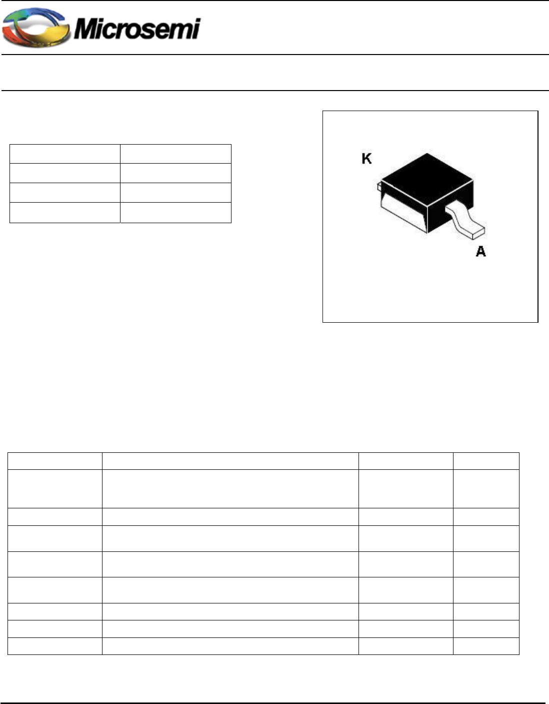
Single schottky rectifier assembled in Powermite 1
®
package which features a full metallic bottom that
eliminates possibility of solder flux entrapment during assembly. The package also incorporates a unique
locking tab which acts as an efficient heat path from die to mounting plane for external heat sinking with
very low thermal resistance junction to case (bottom).
This product is suitable for use in switching and regulating power supplies and also charge pump
circuits.
Absolute maximum ratings
(1)
Symbol Parameter Value Unit
V
RRM
V
RWM
V
R
Peak Repetitive Reverse Voltage
Working Peak Reverse Voltage
DC Blocking Voltage
20 V
V
R(RMS)
RMS Reverse Voltage 14 V
I
O
Average rectified forward output current
(T
C
= 135ºC)
1.0 A
I
FRM
Peak repetitive forward current
(100kHz square wave, T
C
= 135ºC)
2.0 A
I
FSM
Non repetitive peak forward surge current
(8.3ms single half sine wave)
50 A
dV/dt Voltage rate of change (at max V
R
) 10000 V/µs
T
STG
Storage temperature -55 to +150 ºC
T
J
Junction temperature -55 to +125 ºC
(1)
All ratings at 25ºC unless specified otherwise
I
O
1A
V
RRM
20V
T
j(MAX)
125ºC
V
F(MAX)
0.415V
Powermite 1
(DO-216AA)
Schottky Barrier Rectifier
www.Microsemi.com
2/4
Copyright © 2008
June 2008 Rev E
UPS120e3
Characteristics
Static Electrical Characteristics
Symbol Parameter Test Conditions Typ max Units
I
F
= 0.1 A 0.34
I
F
= 1.0 A 0.45
T
J
= 25ºC
I
F
= 3.0 A 0.65
I
F
= 0.1 A 0.25
I
F
= 1.0 A 0.415
V
F
(2)
Maximum forward voltage
T
J
= 85ºC
I
F
= 3.0 A 0.67
V
V
R
= 20V 0.40
T
J
= 25ºC
V
R
= 10V 0.10
V
R
= 20V 25
I
R
(2)
Maximum instantaneous
reverse current
T
J
= 85ºC
V
R
= 10V 18
mA
C
T
Junction capacitance V
R
= 5V, f = 1MHz 80 pF
(2)
Measured with a test pulse of 380µs to minimize self-heating effect
Thermal Characteristics
Symbol Parameter Value Unit
R
ΘJC
Junction to case (bottom) 15 ºC/W
R
ΘJA
Junction to ambient
(3)
240 ºC/W
(3)
Mounted on FR-4 PC board using 1oz copper with recommended minimum foot print
Reverse power dissipation and the possibility of thermal runaway
must be considered when operating this device under any
reverse voltage conditions. Calculations of T
J
therefore must
include forward and reverse power effects. The allowable
operating T
J
may be calculated from the equation:
T
J
= T
J max
= r(t)(Pf+Pr) where
r(t) = thermal impedance under given conditions.
Pf = forward power dissipation, and
Pr = reverse power dissipation
This graph displays the de-rated allowable T
J
due to reverse bias
under DC conditions only and is calculated as T
J
= T
J max
-r(t) Pr,
Where r(t)=Rthja. For other power applications further
calculations must be performed.
Schottky Barrier Rectifier
www.Microsemi.com
3/4
Copyright © 2008
June 2008 Rev E
UPS120e3
Thermal Impedance Junction to Case (bottom)
Thermal Impedance Junction to Ambient
Mechanical Characteristics
Physical dimensions
Dimensions
Millimeters Inches
Ref.
Min. Max. Min. Max.
A
0.73 0.99 0.029 0.039
B
0.40 0.66 0.016 0.026
C
1.77 2.03 0.070 0.080
D
2.21 2.46 0.087 0.097
E
0.50 0.76 0.020 0.030
F
1.29 1.54 0.051 0.061
G
0.53 0.78 0.021 0.031
H
0.10 0.20 0.004 0.008
I
1.77 2.03 0.070 0.080
J
0.89 1.14 0.035 0.045

UPS120/TR7

Mfr. #:
Manufacturer:
Microchip / Microsemi
Description:
Schottky Diodes & Rectifiers Schottky
Lifecycle:
New from this manufacturer.
Delivery:
DHL FedEx Ups TNT EMS
Payment:
T/T Paypal Visa MoneyGram Western Union