DG2018DN-T1-E4

Document Number: 72342
S-82626-Rev. C, 03-Nov-08
www.vishay.com
7
Vishay Siliconix
DG2018, DG2019
TEST CIRCUITS
Figure 1. Switching Time
Switch
Input
C
L
(includes fixture and stray capacitance)
V+
IN
NO or NC
C
L
35 pF
COM
Logic
Input
R
L
300 Ω
V
OUT
GND
V+
50 %
0 V
Logic
Input
Switch
Output
t
ON
t
OFF
Logic "1" = Switch On
Logic input waveforms inverted for switches that have
the opposite logic sense.
0 V
Switch Output
0.9 x V
OUT
t
r
< 5 ns
t
f
< 5 ns
V
INH
V
INL
V
OUT
=V
COM
R
L
R
L
+R
ON
Figure 2. Charge Injection
Off
OnOn
IN
ΔV
OUT
V
OUT
Q = ΔV
OUT
x C
L
C
L
= 1 nF
R
gen
V
OUT
COM
V
IN
= 0 - V+
IN
V
gen
GND
V+
V+
IN depends on switch configuration: input polarity
determined b
y
sense of switch.
+
NC or NO
Figure 3. Break-Before-Make Interval
C
L
(includes fixture and stray capacitance)
NC
V
NO
NO
V
NC
0 V
Logic
Input
Switch
Output
V
O
V
NC
= V
NO
t
r
< 5 ns
t
f
< 5 ns
90 %
t
D
t
D
IN
COM
V+
GND
C
L
35 pF
V
O
R
L
50 Ω
V
INL
V
INH
www.vishay.com
8
Document Number: 72342
S-82626-Rev. C, 03-Nov-08
Vishay Siliconix
DG2018, DG2019
TEST CIRCUITS
Vishay Siliconix maintains worldwide manufacturing capability. Products may be manufactured at one of several qualified locations. Reliability data for Silicon
Technology and Package Reliability represent a composite of all qualified locations. For related documents such as package/tape drawings, part marking, and
reliability data, see http://www.vishay.com/ppg?72342.
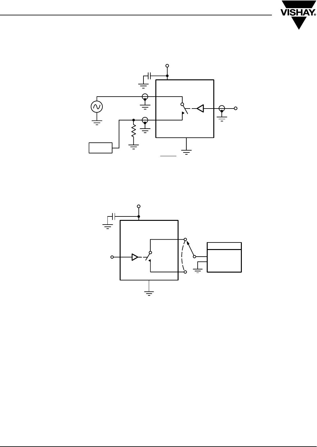
Figure 4. Off-Isolation
IN
GND
NC or NO
0 V, 2.4 V
10 nF
COM
Off Isolation = 20 log
V
COM
V
NO/ NC
R
L
Analyzer
V+
V+
COM
Figure 5. Channel Off/On Capacitance
NC or NO
f = 1 MHz
IN
COM
GND
0 V, 2.4 V
Meter
HP4192A
Impedance
Analyzer
or Equivalent
10 nF
V+
V+
-C-
C0.08
NOTES:
1. All dimensions are in millimeters.
2. N is the total number of terminals.
3. Dimension b applies to metallized terminal and is measured between 0.25 and 0.30 mm from terminal tip.
4. Coplanarity applies to the exposed heat sink slug as well as the terminal.
5. The pin #1 identifier may be either a mold or marked feature, it must be located within the zone iindicated.
4
C0.10//
-A-
-B-
E
SEATING
PLANE
A3
A1A
4
NX
SIDE VIEW
3
3
Terminal Tip
Exposed Pad
D
D/2
E/2
BOTTOM VIEW
TOP VIEW
C0.25
C0.25
E2/2
E2
D2
D2/2
L
e
3 x e
3 x e
C0.10
M
A B
4xb
Package Information
Vishay Siliconix
Document Number: 72208
29-Dec-03
www.vishay.com
1
QFN−16 LEAD (3 X 3)
VARIATION 1 VARIATION 2
Dim MILLIMETERS INCHES MILLIMETERS INCHES
Min Nom Max Min Nom Max Min Nom Max Min Nom Max
A
0.80 0.90 1.00 0.031 0.035 0.039 0.80 0.90 1.00 0.031 0.035 0.039
b
0.18 0.23 0.30 0.007 0.009 0.012 0.18 0.25 0.30 0.007 0.010 0.012
D
3.00 BSC 0.118 BSC 3.00 BSC 0.118 BSC
D2
1.00 1.15 1.25 0.039 0.045 0.049 1.55 1.70 1.80 0.061 0.067 0.071
E
3.00 BSC 0.118 BSC 3.00 BSC 0.118 BSC
E2
1.00 1.15 1.25 0.039 0.045 0.049 1.55 1.70 1.80 0.061 0.067 0.071
e
0.50 BSC 0.020 BSC 0.50 BSC 0.020 BSC
L
0.30 0.40 0.50 0.012 0.016 0.020 0.30 0.40 0.50 0.012 0.016 0.020
ECN: S-32625—Rev. B, 29-Dec-03
DWG: 5899

DG2018DN-T1-E4

Mfr. #:
Manufacturer:
Vishay / Siliconix
Description:
Analog Switch ICs RECOMMENDED ALT 78-DG2523DN-T1-GE4
Lifecycle:
New from this manufacturer.
Delivery:
DHL FedEx Ups TNT EMS
Payment:
T/T Paypal Visa MoneyGram Western Union

Products related to this Datasheet