2
LTC2900
2900f
ORDER PART
NUMBER
MS PART MARKING
LTYJ
LTYL
LTYK
LTYM
T
JMAX
= 125°C, θ
JA
= 250°C/W
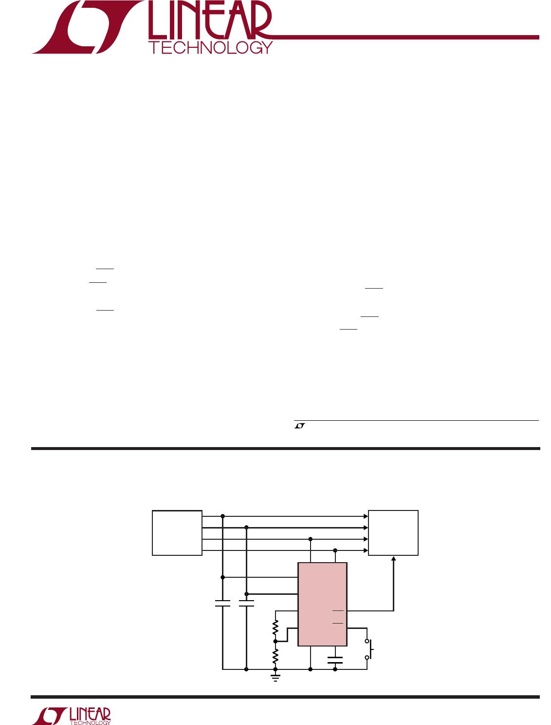
V1, V2, V3, V4, V
PG
, PBR............................. –0.3V to 7V
RST (LTC2900-1)........................................ –0.3V to 7V
RST (LTC2900-2).......................... –0.3V to (V2 + 0.3V)
CRT ............................................. –0.3V to (V
CC
+ 0.3V)
V
REF
............................................. –0.3V to (V
CC
+ 0.3V)
Reference Load Current (I
VREF
) ............................ ±1mA
LTC2900-1CMS
LTC2900-2CMS
LTC2900-1IMS
LTC2900-2IMS
ABSOLUTE AXI U RATI GS
WWWU
PACKAGE/ORDER I FOR ATIO
UU
W
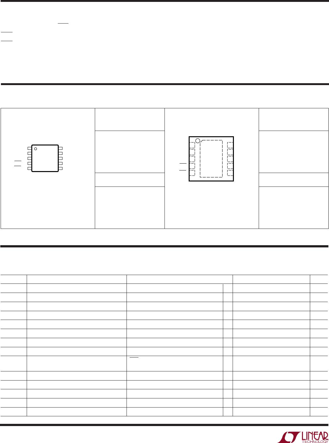
1
2
3
4
5
V3
V1
CRT
RST
PBR
10
9
8
7
6
V2
V4
V
REF
V
PG
GND
TOP VIEW
MS PACKAGE
10-LEAD PLASTIC MSOP
Consult LTC Marketing for parts specified with wider operating temperature ranges.
V4 Input Current (–ADJ Mode) ............................ –1mA
Operating Temperature Range
LTC2900-1C/LTC2900-2C ....................... 0°C to 70°C
LTC2900-1I/LTC2900-2I .................... –40°C to 85°C
Storage Temperature Range .................. –65°C to 150°C
Lead Temperature (Soldering, 10 sec)................... 300°C
(Notes 1, 2, 3)
ORDER PART
NUMBER
DD PART MARKING
LABU
LABW
LABV
LABX
LTC2900-1CDD
LTC2900-2CDD
LTC2900-1IDD
LTC2900-2IDD
T
JMAX
= 125°C, θ
JA
= 43°C/W
SYMBOL PARAMETER CONDITIONS MIN TYP MAX UNITS
V
RT50
5V, 5% Reset Threshold V1 Input Threshold ● 4.600 4.675 4.750 V
V
RT33
3.3V, 5% Reset Threshold V1, V2 Input Threshold ● 3.036 3.086 3.135 V
V
RT30
3V, 5% Reset Threshold V2 Input Threshold ● 2.760 2.805 2.850 V
V
RT25
2.5V, 5% Reset Threshold V2, V3 Input Threshold ● 2.300 2.338 2.375 V
V
RT18
1.8V, 5% Reset Threshold V3, V4 Input Threshold ● 1.656 1.683 1.710 V
V
RT15
1.5V, 5% Reset Threshold V3, V4 Input Threshold ● 1.380 1.403 1.425 V
V
RTA
ADJ Reset Threshold V3, V4 Input Threshold ● 0.492 0.500 0.508 V
V
RTAN
–ADJ Reset Threshold V4 Input Threshold ● –18 0 18 mV
V
CC
Minimum Internal Operating Voltage RST in Correct Logic State, ● 1V
V
CC
Rising Prior to Program
V
CCMINP
Minimum Required for Programming V
CC
Rising ● 2.42 V
V
REF
Reference Voltage V
CC
≥ 2.3V, I
VREF
= ±1mA, C
REF
≤ 1000pF ● 1.192 1.210 1.228 V
V
PG
Programming Voltage Range V
CC
≥ V
CCMINP
● 0V
REF
V
I
VPG
V
PG
Input Current V
PG
= V
REF
● ±20 nA
I
V1
V1 Input Current V1 = 5V, I
VREF
= 12µA, (Note 4) ● 43 75 µA
The ● denotes the specifications which apply over the full operating
temperature range, otherwise specifications are at T
A
= 25°C. V
CC
= 5V, unless otherwise noted. (Note 3)
ELECTRICAL CHARACTERISTICS
TOP VIEW
DD PACKAGE
10-LEAD (3mm × 3mm) PLASTIC DFN
10
9
6
7
8
4
5
3
2
1
V2
V4
V
REF
V
PG
GND
V3
V1
CRT
RST
PBR