11
LTC2900
2900f
APPLICATIO S I FOR ATIO
WUUU
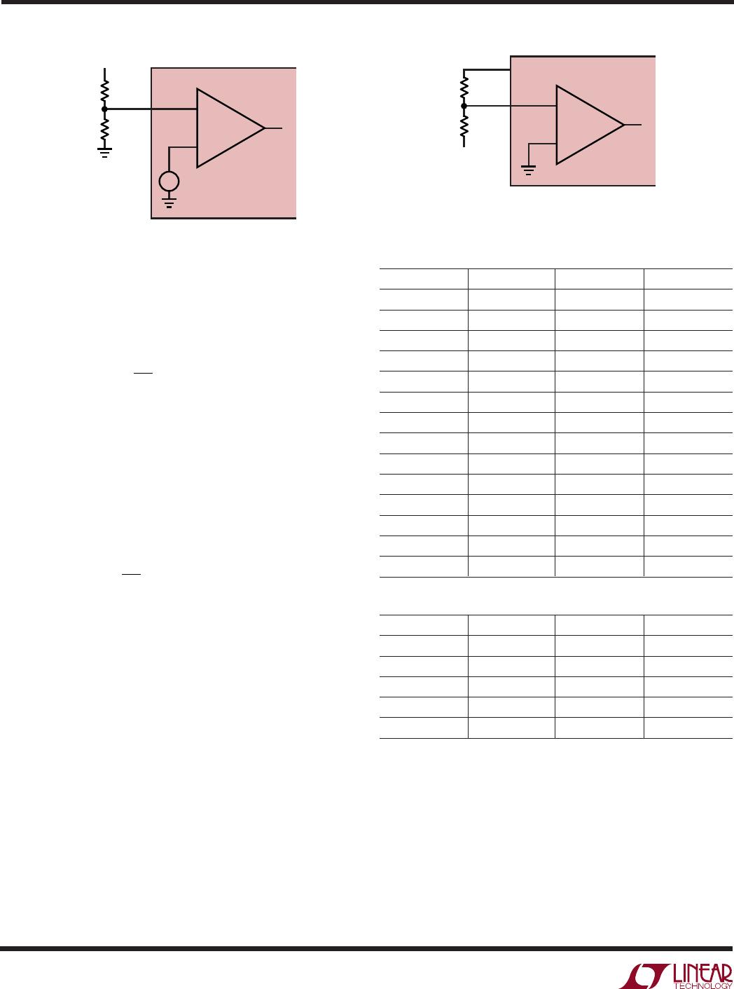
Although all four supply monitor comparators have built-
in glitch immunity, bypass capacitors on V1 and V2 are
recommended because the greater of V1 or V2 is also the
V
CC
for the device. Filter capacitors on the V3 and V4
inputs are allowed.
Power-Down
On power-down, once any of the V
X
inputs drop below
their threshold, RST is held at a logic low. A logic low of
0.4V is guaranteed until both V1 and V2 drop below 1V. If
the bandgap reference becomes invalid (V
CC
< 2V typ), the
part will reprogram once V
CC
rises above 2.4V max.
Monitor Output Rise and Fall Time Estimation
The RST output has strong pull-down capability. If the
external load capacitance (C
LOAD
) is known, output fall
time (10% to 90%) is estimated using:
t
FALL
≈ 2.2 • R
PD
• C
LOAD
where R
PD
is the on-resistance of the internal pull-down
transistor. The typical performance curve (V
OL
vs I
SINK
)
demonstrates that the pull-down current is somewhat
linear versus output voltage. Using the 25°C curve, R
PD
is
estimated to be approximately 40Ω. Assuming a 150pF
load capacitance, the fall time is about 13.2ns.
Although the RST output of the LTC2900-1 is considered
to be “open-drain,” it does have weak pull-up capability
(see RST Pull-Up Current vs V2 curve). Output rise time
(10% to 90%) is estimated using:
t
RISE
≈ 2.2 • R
PU
• C
LOAD
where R
PU
is the on-resistance of the pull-up transistor.
The on-resistance as a function of the V2 voltage at room
temperature is estimated using:
R
V
PU
=Ω
610
21
5
•
–
with V2 = 3.3V, R
PU
is about 260k. Using 150pF for load
capacitance, the rise time is 86µs. If the output needs to
pull up faster and/or to a higher voltage, a smaller
external pull-up resistor may be used. Using a 10k pull-
up resistor, the rise time is reduced to 3.3µs for a 150pF
load capacitance.
The LTC2900-2 has an active pull-up to V2 on the RST
output. The typical performance curve (RST Pull-Up Cur-
rent vs V2 curve) demonstrates that the pull-up current is
somewhat linear versus the V2 voltage and R
PU
is esti-
mated to be approximately 625Ω. A 150pF load capaci-
tance makes the rise time about 206ns.
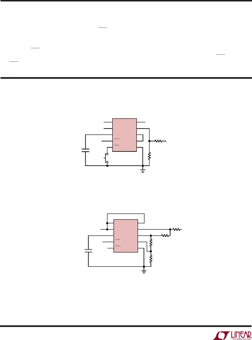
Selecting the Reset Timing Capacitor
The reset time-out period is adjustable in order to accom-
modate a variety of microprocessor applications. The
reset time-out period, t
RST
, is adjusted by connecting a
capacitor, C
RT
, between the CRT pin and ground. The value
of this capacitor is determined by:
C
RT
= t
RST
• 217 • 10
–9
with C
RT
in Farads and t
RST
in seconds. The C
RT
value per
millisecond of delay can also be expressed as C
RT
/ms =
217 (pF/ms).
Leaving the CRT pin unconnected will generate a mini-
mum reset time-out of approximately 50µs. Maximum
reset time-out is limited by the largest available low
leakage capacitor. The accuracy of the time-out period will
be affected by capacitor leakage (the nominal charging
current is 2µA) and capacitor tolerance. A low leakage
ceramic capacitor is recommended.