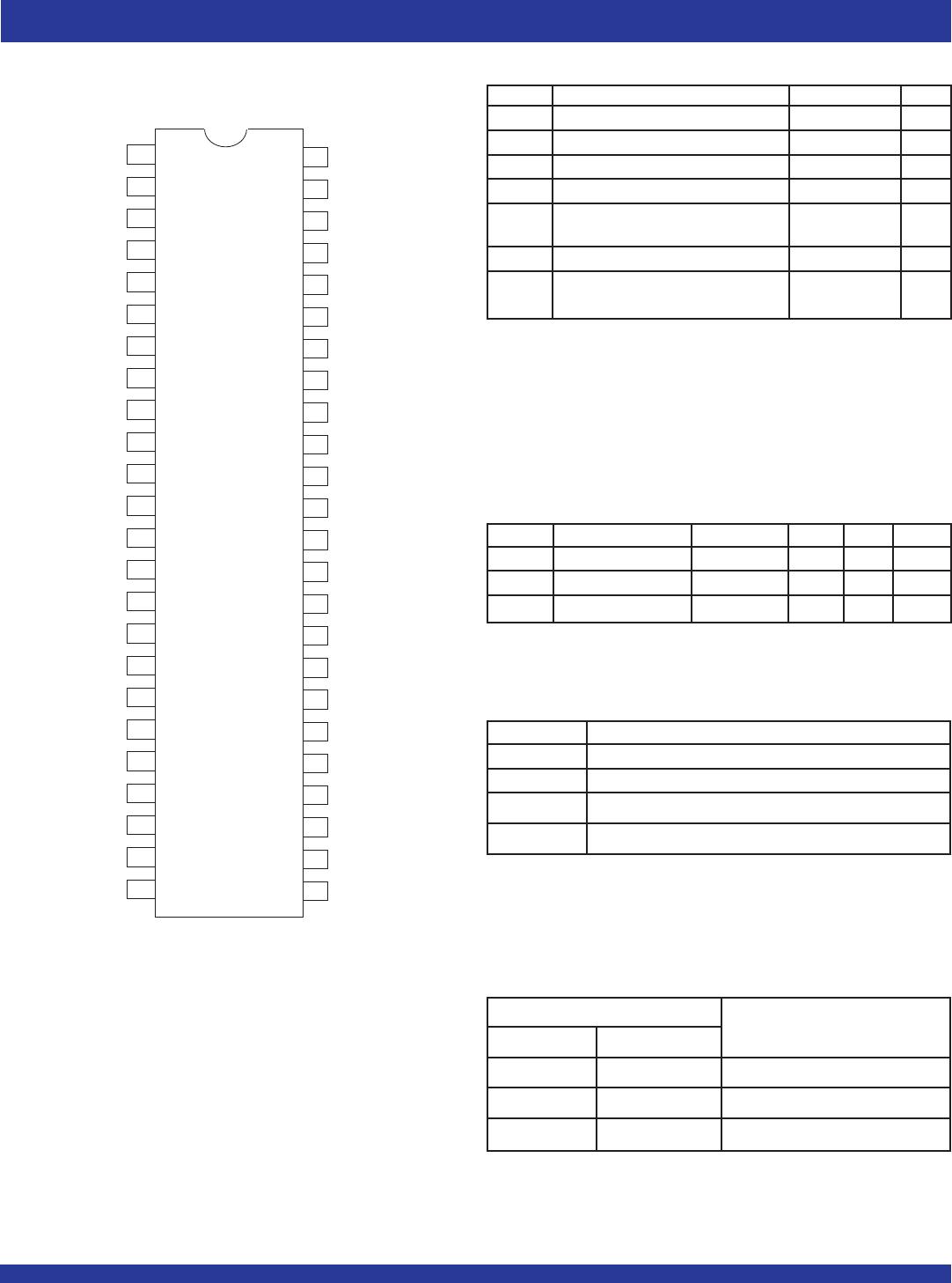
INDUSTRIAL TEMPERATURE RANGE
IDT74ALVCH162245
3.3V CMOS 16-BIT BUS TRANSCEIVER WITH 3-STATE OUTPUTS
1
AUGUST 2016INDUSTRIAL TEMPERATURE RANGE
IDT and the IDT logo are registered trademarks of Integrated Device Technology, Inc.
© 2016 Integrated Device Technology, Inc. DSC-4748/6
FEATURES:
• 0.5 MICRON CMOS Technology
• Typical tSK(o) (Output Skew) < 250ps
• ESD > 2000V per MIL-STD-883, Method 3015; > 200V using
machine model (C = 200pF, R = 0)
•VCC = 3.3V ± 0.3V, Normal Range
•VCC = 2.7V to 3.6V, Extended Range
•VCC = 2.5V ± 0.2V
• CMOS power levels (0.4
μμ
μμ
μ W typ. static)
• Rail-to-Rail output swing for increased noise margin
• Available in TSSOP package
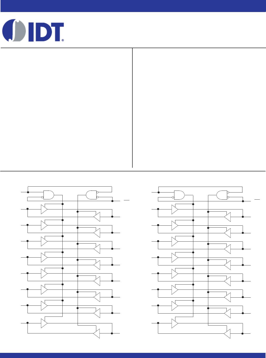
FUNCTIONAL BLOCK DIAGRAM
IDT74ALVCH162245
3.3V CMOS 16-BIT BUS
TRANSCIEVER WITH
3-STATE OUTPUTS
AND BUS-HOLD
DESCRIPTION:
This 16-bit bus transceiver is built using advanced dual metal CMOS
technology. The ALVCH162245 is designed for asynchronous com-
munication between data buses. The control-function implementation
minimizes external timing requirements.
This device can be used as two 8-bit transceivers or one 16-bit
transceiver. It allows data transmission from the A bus to the B bus or
from the B bus to the A bus, depending on the logic level at the
direction-control (DIR) input. The output-enable (OE) input can be
used to disable the device so that the buses are effectively isolated.
The ALVCH162245 has series resistors in the device out-put struc-
ture of the “A” port which will significantly reduce line noise when used
with light loads. This driver has been designed to drive ±12mA at the
designated threshold levels. The “B” port has a ±24mA driver.
The ALVCH162245 has “bus-hold” which retains the inputs’ last
state whenever the input bus goes to a high impedance. This prevents
floating inputs and eliminates the need for pull-up/down resistors.
APPLICATIONS:
• 3.3V high speed systems
• 3.3V and lower voltage computing systems
DRIVE FEATURES:
• Balanced Output Drivers: ±12mA (A port)
• High Output Drivers: ±24mA (B port)
1
DIR
1
A
1
1
A
2
1
A
3
1
A
4
1
A
5
1
A
6
1
A
7
1
A
8
1
B
8
1
B
7
1
B
6
1
B
5
1
B
4
1
B
3
1
B
2
1
B
1
1
OE
2
DIR
2
A
1
2
A
2
2
A
3
2
A
4
2
A
5
2
A
6
2
A
7
2
A
8
2
B
8
2
B
7
2
B
6
2
B
5
2
B
4
2
B
3
2
B
2
2
B
1
2
OE
1
47
46
44
43
41
40
38
37
12
11
9
8
6
5
3
2
48
24
36
35
33
32
30
29
27
26
23
22
20
19
17
16
14
13
25