ADR293
Rev. D | Page 9 of 12
TERMINOLOGY
Line Regulation
The change in output voltage due to a specified change in input
voltage. It includes the effects of self-heating. Line regulation is
expressed in percent per volt, parts per million per volt, or
microvolts per volt change in input voltage.
Load Regulation
The change in output voltage due to a specified change in load
current. It includes the effects of self-heating. Load regulation is
expressed in microvolts per milliampere, parts per million per
milliampere, or ohms of dc output resistance.
Long-Term Stability
Typical shift of output voltage of 25°C on a sample of parts
subjected to high temperature operating life test of 1000 hours
at 125°C.
()
1
OUT
0
OUTOUT
tVtVV =Δ
[]
()
()
()
6
10ppm ×
=Δ
0
OUT
1
OUT
0
OUT
OUT
tV
tVtV
V
where:
V
OUT
(t
0
) = V
OUT
at 25°C at time 0.
V
OUT
(t
1
) = V
OUT
at 25°C after 1000 hours operation at 125°C.
NC = No Connect
There are in fact connections at NC pins, which are reserved for
manufacturing purposes. Users should not connect anything at
NC pins.
Temperature Coefficient
The change of output voltage over the operating temperature
change and normalized by the output voltage at 25°C, expressed
in ppm/°C.
[]
()
)
()
()
6
10Cppm/ ×
×°
=°
12
OUT
1
OUT
2
OUT
OUT
TTC25V
TVΤV
VTC
where:
V
OUT
(25°C) = V
OUT
at 25°C.
V
OUT
(T
1
) = V
OUT
at Temperature 1.
V
OUT
(T
2
) = V
OUT
at Temperature 2.
Thermal Hysteresis
Thermal hysteresis is defined as the change of output voltage
after the device is cycled through temperatures from +25°C to
–40°C to +85°C and back to +25°C. This is a typical value from
a sample of parts put through such a cycle.
)
TCOUTOUTHYSOUT
VC25VV
°
=
[]
()
()
6
10ppm ×
°
°
=
C25V
VC25V
V
OUT
TCOUTOUT
HYSOUT
where:
V
OUT
(25°C) = V
OUT
at 25°C.
V
OUT-TC
= V
OUT
(25°C) after temperature cycle at +25°C to –40°C
to +85°C and back to +25°C.
ADR293
Rev. D | Page 10 of 12
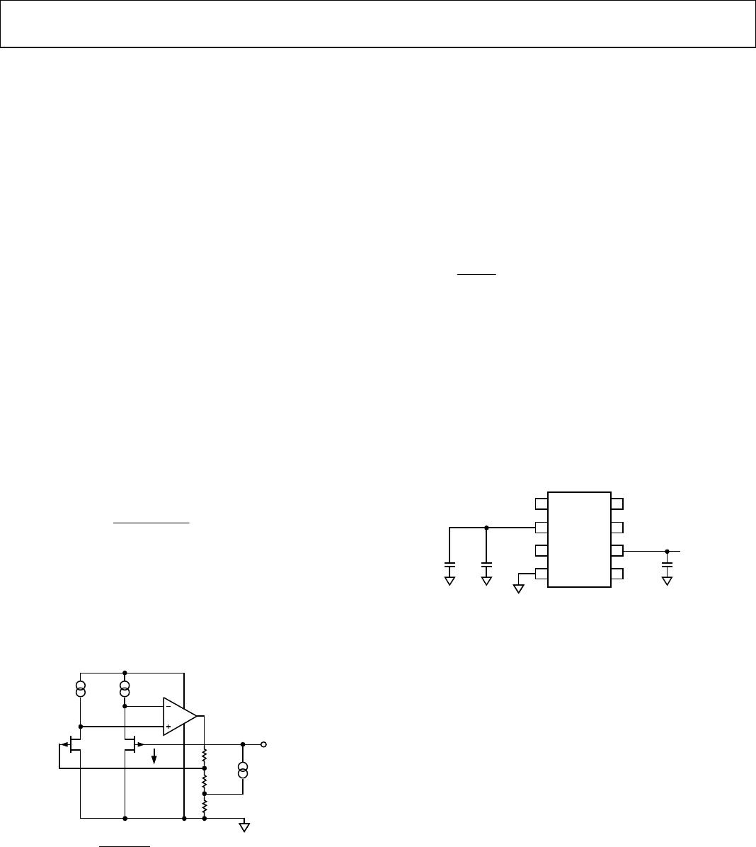
THEORY OF OPERATION
The ADR293 uses a new reference generation technique known
as XFET, which yields a reference with low noise, low supply
current, and very low thermal hysteresis.
The core of the XFET reference consists of two junction field
effect transistors, one of which has an extra channel implant to
raise its pinch-off voltage. By running the two JFETs at the same
drain current, the difference in pinch-off voltage can be amplified
and used to form a highly stable voltage reference. The intrinsic
reference voltage is around 0.5 V with a negative temperature
coefficient of about –120 ppm/K. This slope is essentially locked
to the dielectric constant of silicon and can be closely compen-
sated by adding a correction term generated in the same fashion
as the proportional-to-temperature (PTAT) term used to
compensate band gap references. The big advantage over a band
gap reference is that the intrinsic temperature coefficient is
some 30 times lower (therefore, less correction is needed) and
this results in much lower noise, because most of the noise of a
band gap reference comes from the temperature compensation
circuitry.
The simplified schematic in Figure 21 shows the basic topology
of the ADR293. The temperature correction term is provided by
a current source with value designed to be proportional to
absolute temperature. The general equation is
()
()
R3I
R1
R3R2R1
VV
PTAT
P
OUT
+
++
Δ=
where:
ΔV
P
is the difference in pinch-off voltage between the two FETs.
I
PTAT
is the positive temperature coefficient correction current.
The process used for the XFET reference also features vertical
NPN and PNP transistors, the latter of which are used as output
devices to provide a very low dropout voltage.
V
OUT
V
IN
I
PTAT
GND
R1
R2
R3
I
1
I
1
1
1
EXTRA CHANNEL IMPLANT
V
OUT
V
P
+ I
PTAT
× R3
R1 + R2 + R3
R1
V
P
00164-021
Figure 21. Simplified Schematic
DEVICE POWER DISSIPATION CONSIDERATIONS
The ADR293 is guaranteed to deliver load currents to 5 mA
with an input voltage that ranges from 5.5 V to 15 V. When
this device is used in applications with large input voltages,
care should be exercised to avoid exceeding the published
specifications for maximum power dissipation or junction
temperature that could result in premature device failure.
The following formula should be used to calculate a devices
maximum junction temperature or dissipation:
JA
A
J
D
TT
P
θ
=
where:
T
J
and T
A
are the junction temperature and ambient
temperature, respectively.
P
D
is the device power dissipation.
θ
JA
is the device package thermal resistance.
BASIC VOLTAGE REFERENCE CONNECTIONS
References, in general, require a bypass capacitor connected
from the V
OUT
pin to the GND pin. The circuit in Figure 22
illustrates the basic configuration for the ADR293. Note that the
decoupling capacitors are not required for circuit stability.
NC
NC
NC
NC
V
OUT
NC
0.1µF
0.1µF
10µF
+
NC = NO CONNECT
1
2
3
4
8
7
6
5
00164-022
ADR293
Figure 22. Basic Voltage Reference Configuration
NOISE PERFORMANCE
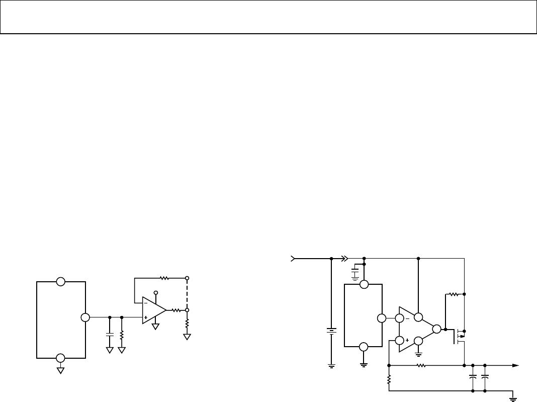
The noise generated by the ADR293 is typically less than
15 μV p-p over the 0.1 Hz to 10 Hz band. The noise measure-
ment is made with a band-pass filter made of a 2-pole high-pass
filter with a corner frequency at 0.1 Hz and a 2-pole low-pass
filter with a corner frequency at 10 Hz.
TURN-ON TIME
Upon application of power (cold start), the time required for
the output voltage to reach its final value within a specified
error band is defined as the turn-on settling time. Two
components normally associated with this are the time for the
active circuits to settle and the time for the thermal gradients on
the chip to stabilize. Figure 15 shows the typical turn-on time
for the ADR293.
ADR293
Rev. D | Page 11 of 12
APPLICATIONS
KELVIN CONNECTIONS
In many portable instrumentation applications where PC board
cost and area go hand-in-hand, circuit interconnects are very often
of dimensionally minimum width. These narrow lines can cause
large voltage drops if the voltage reference is required to provide
load currents to various functions. In fact, a circuit’s interconnects
can exhibit a typical line resistance of 0.45 mΩ/square (1 oz. Cu,
for example). Force and sense connections, also referred to as
Kelvin connections, offer a convenient method of eliminating
the effects of voltage drops in circuit wires. Load currents flowing
through wiring resistance produce an error (V
ERROR
= R × I
L
) at
the load. However, the Kelvin connection in Figure 23 overcomes
the problem by including the wiring resistance within the forcing
loop of the op amp. Because the op amp senses the load voltage,
op amp loop control forces the output to compensate for the
wiring error and to produce the correct voltage at the load.
A1
1µF
100k
+V
OUT
SENSE
V
IN
R
LW
R
L
R
LW
+V
OUT
FORCE
V
OUT
GND
V
IN
ADR293
2
6
4
0
0164-025
Figure 23. Advantage of Kelvin Connection
VOLTAGE REGULATOR FOR PORTABLE
EQUIPMENT
The ADR293 is ideal for providing a stable, low cost, and low
power reference voltage in portable equipment power supplies.
Figure 24 shows how the ADR293 can be used in a voltage
regulator that not only has low output noise (as compared to
switch mode design) and low power, but also a very fast
recovery after current surges. Some precautions should be taken
in the selection of the output capacitors. Too high an ESR
(effective series resistance) could endanger the stability of the
circuit. A solid tantalum capacitor, 16 V or higher, and an
aluminum electrolytic capacitor, 10 V or higher, are recom-
mended for C1 and C2, respectively. In addition, the path from
the ground side of C1 and C2 to the ground side of R1 should
be kept as short as possible.
ADR293
V
OUT
GND
V
IN
0.1µF
LEAD-ACID
BATTERY
+
6V
CHARGER
INPUT
R1
402k
1%
C1
68µF
TANT
C2
1000µF
ELECT
R2
402k
1%
++
5V, 100mA
IRF9530
R3
510k
OP20
2
6 2
7
6
4
3
4
00164-026
Figure 24. Voltage Regulator for Portable Equipment

ADR293ERZ

Mfr. #:
Manufacturer:
Analog Devices Inc.
Description:
Voltage References 5V Micropower Low Noise Prec
Lifecycle:
New from this manufacturer.
Delivery:
DHL FedEx Ups TNT EMS
Payment:
T/T Paypal Visa MoneyGram Western Union