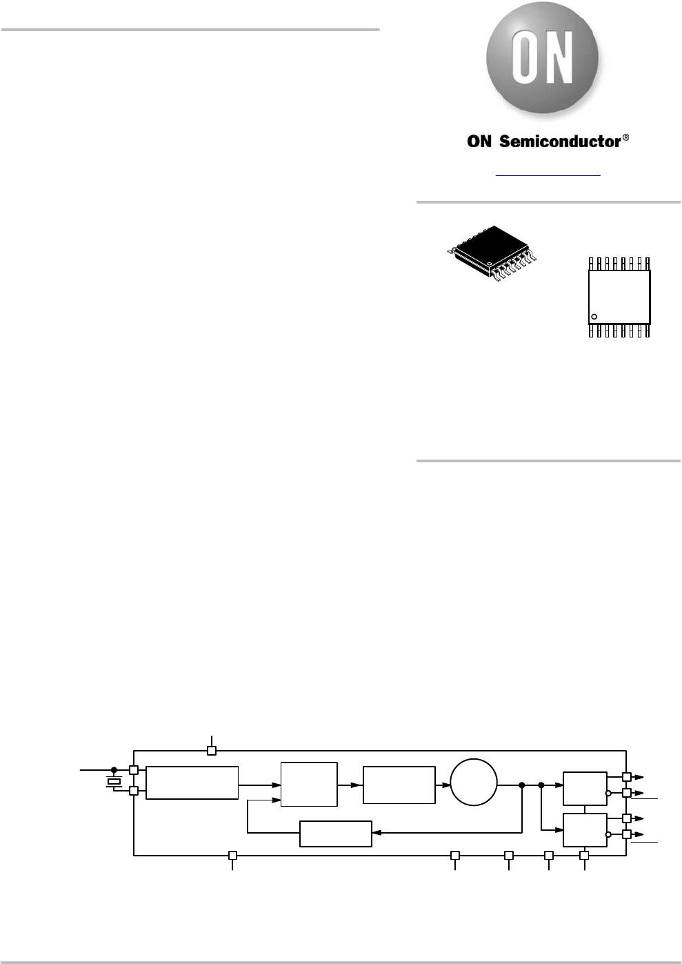
NB3N5573
www.onsemi.com
3
Table 3. ATTRIBUTES
Characteristic Value
ESD Protection Human Body Model > 2 kV
RPU − OE, S0 and S1 Pull−up Resistor
100 kW
Moisture Sensitivity, Indefinite Time Out of Dry Pack (Note 1) Level 1
Flammability Rating Oxygen Index: 28 to 34 UL 94 V−0 @ 0.125 in
Transistor Count 7623
Meets or exceeds JEDEC Spec EIA/JESD78 IC Latchup Test
1. For additional information, see Application Note AND8003/D.
Table 4. MAXIMUM RATINGS (Note 2)
Symbol
Parameter Condition 1 Condition 2 Rating Unit
V
DD
Positive Power Supply GND = 0 V 4.6 V
V
I
Input Voltage (V
IN
) GND = 0 V GND v V
I
v V
DD
−0.5 V to V
DD
+0.5 V V
T
A
Operating Temperature Range −40 to +85 °C
T
stg
Storage Temperature Range −65 to +150 °C
q
JA
Thermal Resistance (Junction−to−Ambient) 0 lfpm
500 lfpm
TSSOP–16
TSSOP–16
138
108
°C/W
°C/W
q
JC
Thermal Resistance (Junction−to−Case) (Note 3) TSSOP−16 33 to 36 °C/W
T
sol
Wave Solder 265 °C
Stresses exceeding those listed in the Maximum Ratings table may damage the device. If any of these limits are exceeded, device functionality
should not be assumed, damage may occur and reliability may be affected.
2. Maximum ratings applied to the device are individual stress limit values (not normal operating conditions) and not valid simultaneously. If
stress limits are exceeded device functional operation is not implied, damage may occur and reliability may be affected.
3. JEDEC standard multilayer board − 2S2P (2 signal, 2 power).
Table 5. DC CHARACTERISTICS (V
DD
= 3.3 V ±10%, GND = 0 V, T
A
= −40°C to +85°C, Note 4)
Symbol Characteristic Min Typ Max Unit
VDD Power Supply Voltage 2.97 3.3 3.63 V
I
DD
Power Supply Current 120 135 mA
I
DDOE
Power Supply Current when OE is Set Low 65 mA
V
IH
Input HIGH Voltage (X/CLK, S0, S1, and OE) 2000 V
DD
+ 300 mV
V
IL
Input LOW Voltage (X/CLK, S0, S1, and OE) GND − 300 800 mV
V
OH
Output HIGH Voltage for HCSL Output (See Figure 5) 660 700 850 mV
V
OL
Output LOW Voltage for HCSL Output (See Figure 5) −150 0 150 mV
V
cross
Crossing Voltage Magnitude (Absolute) for HCSL Output 250 550 mV
DV
cross
Change in Magnitude of V
cross
for HCSL Output 150 mV
NOTE: Device will meet the specifications after thermal equilibrium has been established when mounted in a test socket or printed circuit
board with maintained transverse airflow greater than 500 lfpm.
4. Measurement taken with outputs terminated with R
S
= 33.2 W, R
L
= 49.9 W, with test load capacitance of 2 pF and current biasing resistor
set at 475 W. See Figure 3.