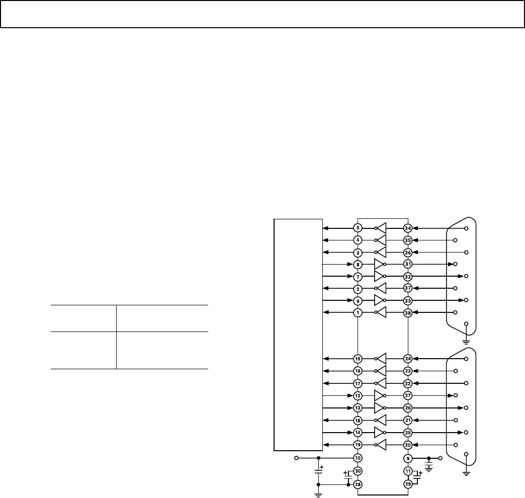
REV. 0
ADM2209E
–9–
(Electrical Fast Transient) discharges. A simplified schematic of
the protection structure is shown in Figures 22a and 22b. Each
input and output contains two back-to-back high speed clamping
diodes. During normal operation with maximum RS-232 signal
levels, the diodes have no effect as one or the other is reverse-
biased, depending on the polarity of the signal. If, however, the
voltage exceeds about ±50 V, reverse breakdown occurs and the
voltage is clamped at this level. The diodes are large p-n junctions
designed to handle the instantaneous current surge which can
exceed several amperes.
The transmitter outputs and receiver inputs have a similar pro-
tection structure. The receiver inputs can also dissipate some of
the energy through the internal 5 k resistor to GND as well as
through the protection diodes.
The protection structure achieves ESD protection up to ±15 kV
and EFT protection up to ±2 kV on all RS-232 I-O lines. The
methods used to test the protection scheme are discussed later.
R
IN
Rx
D1
D2
RECEIVER
INPUT
Figure 22a. Receiver Input Protection Scheme
Tx
TRANSMITTER
OUTPUT
D1
D2
Figure 22b. Transmitter Output Protection Scheme
ESD TESTING (IEC1000-4-2)
IEC1000-4-2 (previously 801-2) specifies compliance testing
using two coupling methods, contact discharge and air-gap
discharge. Contact discharge calls for a direct connection to the
unit being tested. Air-gap discharge uses a higher test voltage
but does not make direct contact with the unit under test. With
air discharge, the discharge gun is moved towards the unit un-
der test developing an arc across the air gap, hence the term air-
discharge. This method is influenced by humidity, temperature,
barometric pressure, distance and rate of closure of the discharge
gun. The contact-discharge method, while less realistic, is more
repeatable and is gaining acceptance in preference to the air-gap
method.
Although very little energy is contained within an ESD pulse,
the extremely fast rise time coupled with high voltages can cause
failures in unprotected semiconductors. Catastrophic destruc-
tion can occur immediately as a result of arcing or heating. Even
if catastrophic failure does not occur immediately, the device
may suffer from parametric degradation, which may result in
degraded performance. The cumulative effects of continuous
exposure can eventually lead to complete failure.
I-O lines are particularly vulnerable to ESD damage. Simply
touching or plugging in an I-O cable can result in a static dis-
charge that can damage or completely destroy the interface
product connected to the I-O port. Traditional ESD test meth-
ods such as the MIL-STD-883B method 3015.7 do not fully
test a product’s susceptibility to this type of discharge. This test
was intended to test a product’s susceptibility to ESD damage
during handling. Each pin is tested with respect to all other
pins. There are some important differences between the tradi-
tional test and the IEC test:
(a) The IEC test is much more stringent in terms of discharge
energy. The peak current injected is over four times greater.
(b) The current rise time is significantly faster in the IEC test.
(c) The IEC test is carried out while power is applied to the device.
It is possible that the ESD discharge could induce latch-up in the
device under test. This test is therefore more representative of a
real-world I-O discharge where the equipment is operating nor-
mally with power applied. For maximum peace of mind, however,
both tests should be performed, to ensure maximum protection
both during handling and later, during field service.
R1 R2
C1
DEVICE
UNDER TEST
HIGH
VOLTAGE
GENERATOR
ESD TEST METHOD R2 C1
H. BODY MIL-STD-883B 1.5kV 100pF
IEC1000-4-2 330V 150pF
Figure 23. ESD Test Standards
100
I
PEAK
– %
90
36.8
10
t
DL
t
RL
TIME t
Figure 24. Human Body Model ESD Current Waveform
100
I
PEAK
– %
90
10
TIME t
30ns
60ns
0.1 TO 1ns
Figure 25. IEC1000-4-2 ESD Current Waveform
REV. 0
ADM2209E
–10–
The ADM2209E is tested using both of the above-mentioned
test methods. All pins are tested with respect to all other pins as
per the MIL-STD-883B specification. In addition, all I-O pins
are tested as per the IEC test specification. The products were
tested under the following conditions:
(a) Power-On—Normal Operation
(b) Power-Off
There are four levels of compliance defined by IEC1000-4-2.
The ADM2209E meets the most stringent compliance level for
both contact and air-gap discharge. This means that the products
are able to withstand contact discharges in excess of 8 kV and air-
gap discharges in excess of 15 kV.
Table IV. IEC1000-4-2 Compliance Levels
Contact Discharge Air Discharge
Level kV kV
12 2
24 4
36 8
48 15
Table V. ADM2209E ESD Test Results
ESD Test Method I-O Pins Other Pins
MIL-STD-883B ±15 kV ±2.5 kV
IEC1000-4-2
Contact ±8 kV
Air ±15 kV
FAST TRANSIENT BURST TESTING (IEC1000-4-4)
IEC1000-4-4 (previously 801-4) covers electrical fast-transient/
burst (EFT) immunity. Electrical fast transients occur as a
result of arcing contacts in switches and relays. The tests simu-
late the interference generated when, for example, a power relay
disconnects an inductive load. A spark is generated due to the
well-known back EMF effect. In fact the spark consists of a burst
of sparks as the relay contacts separate. The voltage appearing
on the line, therefore, consists of a burst of extremely fast tran-
sient impulses. A similar effect occurs when switching on fluo-
rescent lights.
The fast transient burst test defined in IEC1000-4-4 simulates
this arcing and its waveform is illustrated in Figure 26. It con-
sists of a burst of 2.5 kHz to 5 kHz transients repeating at
300 ms intervals. It is specified for both power and data lines.
300ms 15ms
t
V
5ns
0.2/0.4ms
50ns
V
t
Figure 26. IEC1000-4-4 Fast Transient Waveform
Table VI.
V Peak (kV) V Peak (kV)
Level PSU I-O
1 0.5 0.25
2 1 0.5
321
442
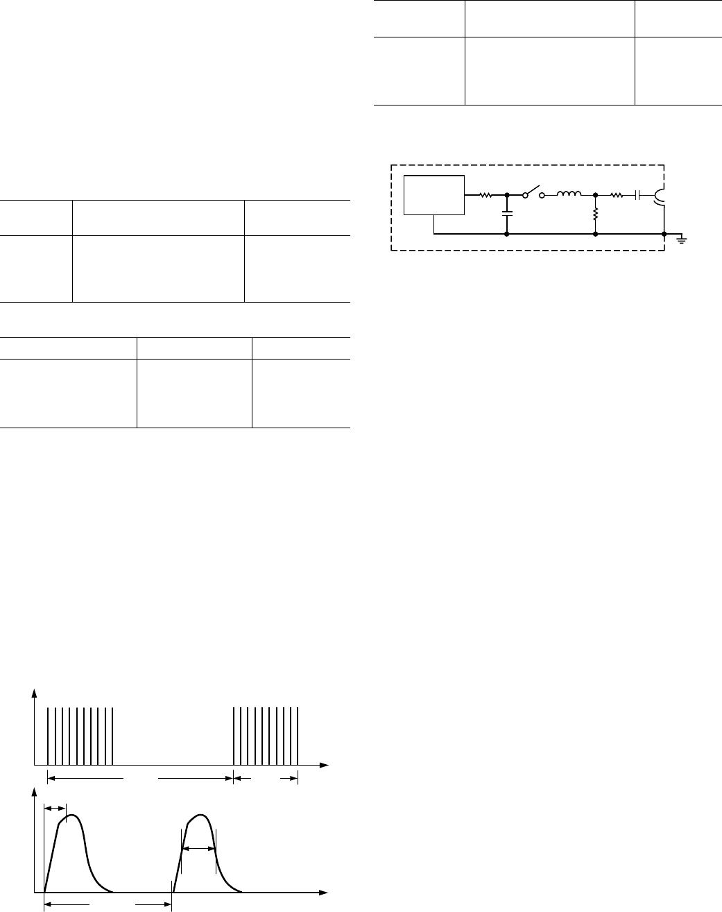
A simplified circuit diagram of the actual EFT generator is
illustrated in Figure 27.
R
C
R
M
C
C
HIGH
VOLTAGE
SOURCE
L
Z
S
C
D
50V
OUTPUT
Figure 27. IEC1000-4-4 Fast Transient Generator
The transients are coupled onto the signal lines using an EFT
coupling clamp. The clamp is 1 meter long and it completely
surrounds the cable, providing maximum coupling capacitance
(50 pF to 200 pF typ) between the clamp and the cable. High
energy transients are capacitively coupled onto the signal lines.
Fast rise times (5 ns) as specified by the standard result in very
effective coupling. This test is very severe since high voltages
are coupled onto the signal lines. The repetitive transients can
often cause problems where single pulses do not. Destructive
latch-up may be induced due to the high energy content of the
transients. Note that this stress is applied while the interface
products are powered up and transmitting data. The EFT test
applies hundreds of pulses with higher energy than ESD. Worst
case transient current on an I-O line can be as high as 40 A.
Test results are classified according to the following:
1. Normal performance within specification limits.
2. Temporary degradation or loss of performance which is self-
recoverable.
3. Temporary degradation or loss of function or performance
which requires operator intervention or system reset.
4. Degradation or loss of function which is not recoverable due
to damage.
The ADM2209E has been tested under worst case conditions
using unshielded cables and meets Classification 2. Data trans-
mission during the transient condition is corrupted, but it may
be resumed immediately following the EFT event without user
intervention.
IEC1000-4-3 RADIATED IMMUNITY
IEC1000-4-3 (previously IEC801-3) describes the measure-
ment method and defines the levels of immunity to radiated
electromagnetic fields. It was originally intended to simulate the
electromagnetic fields generated by portable radio transceivers
or any other device that generates continuous wave radiated
electromagnetic energy. Its scope has since been broadened to
include spurious EM energy which can be radiated from fluores-
cent lights, thyristor drives, inductive loads, etc.
REV. 0
ADM2209E
–11–
Testing for immunity involves irradiating the device with an EM
field. There are various methods of achieving this, including use
of an echoic chamber, stripline cell, TEM cell, GTEM cell. A
stripline cell consists of two parallel plates with an electric field
developed between them. The device under test is placed within
the cell and exposed to the electric field. There are three severity
levels having field strengths ranging from 1 V to 10 V/m. Results
are classified in a fashion similar to those for IEC1000-4-4.
1. Normal operation.
2. Temporary degradation or loss of function that is self-
recoverable when the interfering signal is removed.
3. Temporary degradation or loss of function that requires
operator intervention or system reset when the interfering
signal is removed.
4. Degradation or loss of function that is not recoverable due to
damage.
The ADM2209E easily meets Classification 1 at the most strin-
gent (Level 3) requirement. In fact, field strengths up to 30 V/m
showed no performance degradation and error-free data trans-
mission continued even during irradiation.
Table VII. Test Severity Levels (IEC1000-4-3)
Field Strength
Level V/m
11
23
310
EMISSIONS/INTERFERENCE
EN55 022, CISPR22 defines the permitted limits of radiated
and conducted interference from Information Technology (IT)
equipment. The objective of the standard is to minimize the
level of emissions, both conducted and radiated.
APPLICATIONS INFORMATION
In a typical Data Terminal Equipment (DTE) to Data Circuit
Terminating Equipment (DCE) 9-lead de facto interface imple-
mentation, two data lines (TxD and RxD) and six control lines
(RTS, DTR, DSR, CTS and RI) are required. With its six
drivers and ten receivers, the ADM2209E offers a single-chip
solution for the two RS-232 ports normally supplied as standard
in a desktop or notebook personal computer, as shown in Figure
28. The flow-through pinout of the device allows for a very
simple PCB layout, and allows a ground plane to be placed
beneath the IC, and ground lines to be inserted between the
signal lines to minimize crosstalk, without the complication of
multilayer PCBs.
Note that the two receivers kept active by the standby supply
(R5
IN
A and R5
IN
B) should be connected to the Ring In (RI)
line, so that the system can be awakened when a peripheral
device begins to communicate.
FAIL-SAFE RECEIVER OUTPUTS
The ADM2209E has fail-safe receiver outputs that assume a
high output level if the receiver input is zero or open-circuit.
LAPLINK COMPATIBILITY
The ADM2209E can operate up to 460 kbps data rate under
maximum driver load conditions of C
L
= 1000 pF and
R
L
= 3 k at minimum power supply voltages.
SUPER I/O
CHIP
DCD
DSR
RxD
RTS
TxD
CTS
DTR
RI
DCD
DSR
RxD
RTS
TxD
CTS
DTR
RI
1
2
3
4
5
6
8
9
DCD
DSR
RxD
RTS
TxD
CTS
DTR
RI
DCD
DSR
RxD
RTS
TxD
CTS
DTR
RI
0.1mF
+12V
+3V or +5V
9-WAY D
CONNECTOR
COM2
9-WAY D
CONNECTOR
COM1
7
1
2
3
4
5
6
8
9
7
R1
T3
R3
R2
T1
T2
R4
R5
T3
R3
R2
T1
T2
R4
R1
R5
ADM2209E
0.1mF
0.1mF
0.1mF
Figure 28. Typical Application for a Dual Serial Port

ADM2209EARUZ

Mfr. #:
Manufacturer:
Analog Devices Inc.
Description:
RS-232 Interface IC Dual-Port 6 Tx/10 Rx
Lifecycle:
New from this manufacturer.
Delivery:
DHL FedEx Ups TNT EMS
Payment:
T/T Paypal Visa MoneyGram Western Union