ADVFC32KN/+

REV. B
–3–
ADVFC32
UNIPOLAR V/F, POSITIVE INPUT VOLTAGE
When operated as a V/F converter, the transformation from
voltage to frequency is based on a comparison of input signal
magnitude to the 1 mA internal current source.
A more complete understanding of the ADVFC32 requires a
close examination of the internal circuitry of this part. Consider
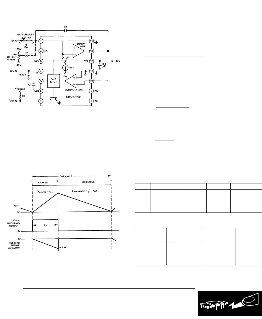
the operation of the ADVFC32 when connected as shown in
Figure 1. At the start of a cycle, a current proportional to the
Figure 1. Connection Diagram for V/F Conversion,
Positive Input Voltage
input voltage flows through R3 and R1 to charge integration
capacitor C2. As charge builds up on C2, the output voltage of
the input amplifier decreases. When the amplifier output volt-
age (Pin 13) crosses ground (see Figure 2 at time t
1
), the
comparator triggers a one shot whose time period is determined
by capacitor C1. Specifically, the one shot time period (in nano-
seconds) is:
t
OS
(C
l
+ 44 pF) × 6.7 k
Figure 2. Voltage-to-Frequency Conversion Waveforms
During this period, a current of (1 mA – I
IN
) flows out of the
integration capacitor. The total amount of charge depleted
during one cycle is, therefore (1 mA – I
IN
) × t
OS
. This charge is
replaced during the remainder of the cycle to return the integra-
tor to its original voltage. Since the charge taken out of C2 is
equal to the charge that is put on C2 every cycle,
(1 mA – I
IN
)
×
t
OS
= I
IN
×
1
F
OUT
t
OS
or, rearranging terms,
F
OUT
=
I
IN
1 mA × t
OS
The complete transfer equation can now be derived by substi-
tuting I
IN
= V
IN
/R
IN
and the equation relating C1 and t
OS
. The
final equation describing ADVFC32 operation is:
V
IIN
/ R
IN
1mA × C
1
+ 44 pF
()
× 6.7 k
Components should be selected to optimize performance over
the desired input voltage and output frequency range using the
equations listed below:
3.7 ×10
7
pF / sec
F
OUT FS
44 pF
C
2
=
10
4
Farads / sec
F
OUT FS
1000 pF minimum
()
R
IN
=
V
IN FS
0.25 mA
R
2
+V
LOGIC
8 mA
Both R
IN
and C
1
should have very low temperature coefficients
as changes in their values will result in a proportionate change
in the V/F transfer function. Other component values and tem-
perature coefficients are not critical.
Table I. Suggested Values for C
1
, R
IN
and C
2
V
IN FS
F
OUT FS
C
1
R
IN
C
2
1 V 10 kHz 3650 pF 4.0 k 0.01 µF
10 V 10 kHz 3650 pF 40 k 0.01 µF
1 V 100 kHz 330 pF 4.0 k 1000 pF
10 V 100 kHz 330 pF 40 k 1000 pF
ORDERING GUIDE
Part Gain Tempco Temp Range Package
Number
1
ppm/C C Option
ADVFC32KN ±75 typ 0 to 70 14-Pin
Plastic DIP
ADVFC32BH ±100 max 25 to +85 TO-100
ADVFC32SH ±150 max 55 to +125 TO-100
NOTE
1
For details on grade and package offerings screened in accordance with MIL-STD-883,
refer to the Analog Devices Military Products Databook or current ADVFC32/883B
data sheet.
CAUTION
ESD (electrostatic discharge) sensitive device. Electrostatic charges as high as 4000 V readily
accumulate on the human body and test equipment and can discharge without detection. Although
the ADVFC32 features proprietary ESD protection circuitry, permanent damage may occur on
devices subjected to high-energy electrostatic discharges. Therefore, proper ESD precautions are
recommended to avoid performance degradation or loss of functionality.
WARNING!
ESD SENSITIVE DEVICE
REV. B
ADVFC32
–4–
Input resistance R
IN
is composed of a fixed resistor (R1) and a
variable resistor (R3) to allow for initial gain error compensa
tion.
To cover all possible situations, R3 should be 20% of R
IN
, and
R1 should be 90% of R
IN
. This allows a ±10% gain adjustment
to compensate for the ADVFC32 full-scale error and the toler-
ance of C1.
If more accurate initial offset is required, the circuit of R4 and
R5 can be added. R5 can have a value between 10 k and
100 k, and R4 should be approximately 10 M. The amount
of current required to trim zero offset will be relatively small, so
the temperature coefficients of these resistors are not critical. If
large offsets are added using this circuit, temperature drift of
both of these resistors is much more important.
BIPOLAR V/F
By adding another resistor from Pin 1 (Pin 2 of TO-100 can) to
a stable positive voltage, the ADVFC32 can be operated with a
bipolar input voltage. For example, an 80 k resistor to 10 V
causes an additional current of 0.125 mA to flow into the inte-
grator so that the net current flow to the integrator is positive
even for negative input voltages. At negative full-scale input
voltage, 0.125 mA will flow into the integrator from V
IN
cancel-
ling out the 0.125 mA from the offset resistor, resulting in an
output frequency of zero. At positive full scale, the sum of the
two currents will be 0.25 mA and the output will be at its maxi-
mum frequency.
UNIPOLAR V/F, NEGATIVE INPUT VOLTAGE
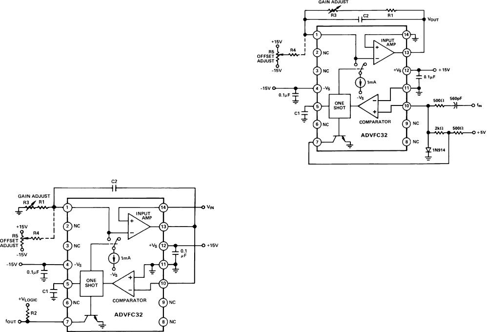
Figure 3 shows the connection diagram for V/F conversion of
negative input voltages. In this configuration full-scale output
frequency occurs at negative full-scale input, and zero output
frequency corresponds to zero input voltage.
Figure 3. Connection Diagram for V/F Conversion,
Negative Input Voltage
A very high impedance signal source may be used since it only
drive the noninverting integrator input. Typical input imped-
ance at this terminal is 250 M or higher. For V/F conversion
of positive input signals the signal generator must be able to
source 0.25 mA to properly drive the ADVFC32, but for nega-
tive V/F conversion the 0.25 mA integration current is drawn
from ground through R1 and R3.
Circuit operation for negative input voltages is very similar to
positive input unipolar conversion described in the previous
section. For best operating results use component equations
listed in that section.
F/V CONVERSION
Although the mathematics of F/V conversion can be very com-
plex, the basic principle is easy to understand. Figure 4 shows
the connection diagram for F/V conversion with TTL input
logic levels. Each time the input signal crosses the comparator
threshold going negative, the one shot is activated and switches
1 mA into the integrator input for a measured time period
(determined by C1). As the frequency increases, the amount of
charge injected into the integration capacitor increases propor-
tionately. The voltage across the integration capacitor is stabilized
when the leakage current through R1 and R3 equals the average
current being switched into the integrator. The net result of
these two effects is an average output voltage which is propor-
tional to the input frequency. Optimum performance can be
obtained by selecting components using the same guidelines and
equations listed in the V/F conversion section.
Figure 4. Connection Diagram for F/V Conversion, TTL
Input
DECOUPLING
Decoupling power supplies at the device is good practice in any
system, but absolutely imperative in high resolution applica-
tions. For the ADVFC32, it is important to remember where
the voltage transients and ground currents flow. For example,
the current drawn through the output pull-down transistor
originates from the logic supply, and is directed to ground
through Pin 11 (Pin 8 of TO-100). Therefore, the logic supply
should be decoupled near the ADVFC32 to provide a low im-
pedance return path for switching transients. Also, if there is a
separate digital ground it should be connected to the analog
ground at the ADVFC32. This will prevent ground offsets that
could be created by directing the full 8 mA output current into
the analog ground, and subsequently back to the logic supply.
Although some circuits may operate satisfactorily with the power
supplies decoupled at only one location on each board, this
practice is not recommended for the ADVFC32. For best results,
each supply should be decoupled with 0.1 µF capacitor at the
ADVFC32. In addition, a larger board level decoupling capaci-
tor of 1 µF to 10 µF should be located relatively close to the
ADVFC32 on each power supply.
COMPONENT TEMPERATURE COEFFICIENTS
The drift specifications of the ADVFC32 do not include tem-
perature effects of any of the supporting resistors or capacitors.
The drift of the input resistors R1 and R3 and the timing capaci-
tor C1 directly affect the overall temperature stability. In the
REV. B
ADVFC32
–5–
application of Figure 2, a 10 ppm/°C input resistor used with a
100 ppm/°C capacitor may result in a maximum overall circuit
gain drift of:
100 ppm/°C (ADVFC32BH) + 100 ppm/°C (C1)
+ 10 ppm/°C (R
IN
) = 210 ppm/°C
Although R
IN
and C1 have the most pronounced effect on tem-
perature stability, the offset circuit of resistors R4 and R5 may
also have a slight effect on the offset temperature drift of the
circuit. The offset will change with variations in the resistance of
R4 and supply voltage changes. In most applications the offset
adjustment is very small, and the offset drift attributable to this
circuit will be negligible. In the bipolar mode, however, both the
positive reference and the resistor used to offset the signal range
will have a pronounced effect on offset drift. A high quality refer-
ence and resistor should be used to minimize offset drift errors.
Other circuit components do not directly influence temperature
performance as long as their actual values are not so different
from nominal value as to preclude operation. This includes
integration capacitor C2. A change in the capacitance value of
C2 results in a different rate of voltage change across C2, but
this is compensated by an equal effect when C2 is discharged
by the switched 1 mA current source so that no net effect occurs.
The temperature effects of the components described above are
the same when the ADVFC32 is configured for negative or
bipolar input ranges, or F/V conversion.
OTHER CIRCUIT CONSIDERATIONS
The input amplifier connected to Pins 1, 13, and 14 is not a
standard operational amplifier. Although it operates like an op
amp in most applications, two key differences should be noted.
First, the bias current of the positive input is typically 40 nA
while the bias current of the inverting input is ±8 nA. Therefore,
any attempt to cancel input offset voltage due to bias currents
by matching input resistors will create worse offsets. Second, the
output of this amplifier will sink only 1 mA, even though it will
source as much as 10 mA. When used in the F/V mode, the
amplifier must be buffered if large sink currents are required.
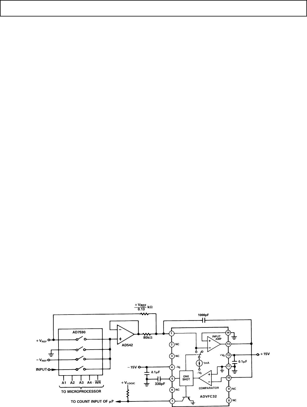
MICROPROCESSOR OPERATED A/D CONVERTER
With the addition of a few external components the ADVFC32
can be used as a ±10 V A/D microprocessor front end. Although
the nonlinearity of the ADVFC32 is only 0.05% maximum
(0.01% typ), the resolution is much higher, allowing it to be
used in 16-bit measurement and control systems where a mono-
tonic transfer function is essential. The resolution of the circuit
shown in Figure 5 is dependent on the amount of time allowed
to count the ADVFC32 frequency output. Using a full-scale
frequency of 100 kHz, an 8-bit conversion can be made in about
10 ms, and a 2 second time period allows a 16-bit measurement,
including offset and gain calibration cycles.
As shown in Figure 5, the input signal is selected via the AD7590
input multiplexer. Positive and negative references as well as a
ground input are provided to calibrate the A/D. This is very
important in systems subject to moderate or extreme temperature
changes since the gain temperature coefficient of the ADVFC32
is as high as ±150 ppm/°C. By using the calibration cycles, the
A/D conversion will be as accurate as the references provided.
The AD542 following the input multiplexer provides a high
impedance input (10
12
ohms) and buffers the switch resistance
from the relatively low impedance ADVFC32 input.
If higher linearity is required, the ADVFC32 can be operated at
10 kHz, but this will require a proportionately longer conversion
time. Conversely, the conversion time can be decreased at the
expense of nonlinearity by increasing the maximum frequency to
as high as 500 kHz.
HIGH NOISE IMMUNITY, HIGH CMRR ANALOG
DATA LINK
In many applications, a signal must be sensed at a remote site
and sent through a very noisy environment to a central location
for further processing. In these cases, even a shielded cable may
not protect the signal from noise pickup. The circuit of Figure 6
provides a solution in these cases. Due to the optocoupler and
voltage-to-frequency conversion, this data link is extremely
insensitive to noise and common-mode voltage interference. For
even more protection, an optical fiber link substituted for the
HCPL2630 will provide common-mode rejection of more than
several hundred kilovolts and virtually total immunity to electrical
noise. For most applications, however, the frequency modulated
signal has sufficient noise immunity without using an optical
fiber
link, and the optocoupler provides common-mode isolation up
to 3000 V dc.
Figure 5. High Resolution, Self-Calibrating, Microprocessor Operated A/D Converter

ADVFC32KN/+

Mfr. #:
Manufacturer:
Analog Devices Inc.
Description:
Voltage to Frequency & Frequency to Voltage V/F Converter IC
Lifecycle:
New from this manufacturer.
Delivery:
DHL FedEx Ups TNT EMS
Payment:
T/T Paypal Visa MoneyGram Western Union

Products related to this Datasheet