3 www.fairchildsemi.com
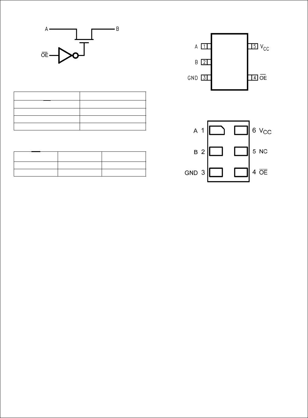
NC7SZD384
Absolute Maximum Ratings(Note 1)
Recommended Operating
Conditions
(Note 3)
Note 1: The “Absolute Maximum Ratings” are those values beyond which the safety
of the device cannot be guaranteed. The device should not be operated at these lim-
its. The parametric values defined in the Electrical Characteristics tables are not
guaranteed at the absolute maximum ratings. The “Recommended Operating Condi-
tions” table will define the conditions for actual device operation.
Note 2: The input and output negative voltage ratings may be exceeded if the input
and output diode current ratings are observed.
Note 3: Unused inputs must be held HIGH or LOW. They may not float.
DC Electrical Characteristics
Note 4: All typical values are at V
CC
5.0V, T
A
25 C.
Note 5: Measured by the voltage drop between A and B pins at the indicated current through the switch. On Resistance is determined by the lower of the voltages on the two (A
or B) pins.
Note 6: Per TTL driven input (V
IN
3.4V, control input only). A and B pins do not contribute to I
CC.
Supply Voltage (V
CC
) 0.5V to 7.0V
DC Switch Voltage (VS)
0.5V to 7.0V
DC Input Voltage (V
IN
) (Note 2) 0.5V to 7.0V
DC Input Diode Current (I
IK
) V
IN
0V 50 mA
DC Output (I
OUT
) Sink Current 128 mA
DC V
CC
/GND Current (I
CC
/GND) 100 mA
Storage Temperature Range (T
STG
) 65 C to 150 C
Junction Temperature under bias (T
J
) 150 C
Junction Lead Temperature (T
L
)
(Soldering, 10 seconds)
260 C
Power Dissipation (P
D
) @ 85 C
SOT23-5 200 mW
SC70-5 150 mW
Power Supply Operating (V
CC
) 4.5V to 5.5V
Input Voltage (V
IN
) 0V to 5.5V
Output Voltage (V
OUT
) 0V to 5.5V
Input Rise and Fall Time (t
r
, t
f
)
Switch Control Input 0 ns/V to 5 ns
Switch I/O 0 ns/V to DC
Operating Temperature (T
A
) 40 C to 85 C
Thermal Resistance (
JA
)
SOT23-5 300
C/Watt
SC70-5 425
C/Watt
Symbol Parameter
V
CC
T
A
40 C to 85 C
Units Conditions
(V)
Min Typ
(Note 4)
Max
V
IK
Maximum Clamp Diode Voltage 4.5 1.2 VI
IN
18 mA
V
IH
HIGH Level Input Voltage 4.5–5.5 2.0 V
V
IL
LOW Level Input Voltage 4.5–5.5 0.8 V
V
OH
HIGH Level Output Voltage 4.5–5.5 See Figure 3 V V
IN
V
CC
I
I
Input Leakage Current 0–5.5 1.0 A0 V
IN
5.5V
I
OFF
“OFF” Leakage Current 5.5 10.0 A0 A, B, V
CC
R
ON
Switch On Resistance (Note 5) 4.5 5.0 7.0 V
IN
0V, I
I
64 mA
5.0 7.0 V
IN
0V, I
I
30 mA
35.0 50.0 V
IN
2.4V, I
I
15 mA
I
CC
Quiescent Supply Current V
IN
V
CC
or GND, I
O
0
Switch On 5.5 0.8 1.5 mA OE
GND
Switch Off 5.5 10.0 AOE
V
CC
I
CC
Increase in I
CC
per Input (Note 6) 5.5 0.8 2.5 mA OE 3.4V, I
O
0,
Control Input only.