NCP1622
www.onsemi.com
17
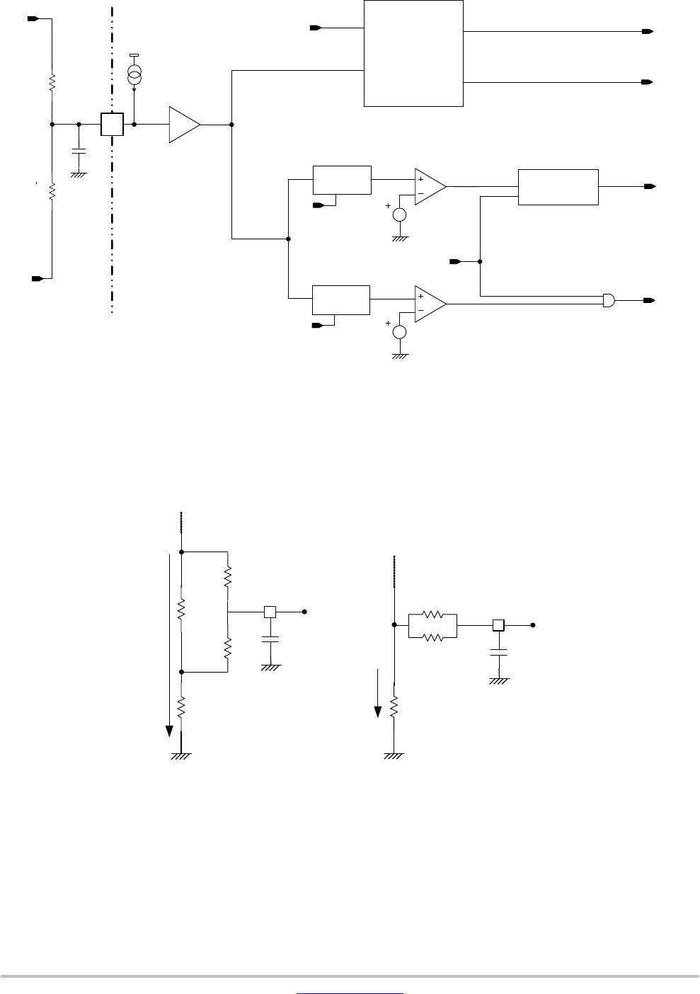
During the On−time and after a 200 ns blanking time, an
OCP (Over Current Protection) signal is generated by an
OCP comparator, comparing (V
CS
= V
CS2
) to a 500 mV
internal reference.
When R
sense
I
ds_max
= V
CS
= V
CS2
= 500 mV we get:
I
ds_max
+
V
ocp
R
sense
(eq. 4)
When V
CS
exceeds the 500 mV internal reference
threshold, the OCP signal turns high to reset the PWM latch
and forces the driver low. The 200 ns blanking time prevents
the OCP comparator from tripping because of the switching
spikes that occur when the MOSFET turns on.
Zero Current Detection
The CS pin is also designed to receive, during t
DEMAG
and
t
DT
, a scaled down (divided by 138) power MOSFET drain
voltage that will be used for Zero Current Detection. It may
happen that the MOSFET turns on while a huge current
flows through the inductor. As an example such a situation
can occur at start−up when large in−rush currents charge the
bulk capacitor to the line peak voltage. Traditionally, a
bypass diode is generally placed between the input and
output high−voltage rails to divert this inrush current. If this
diode is accidently shorted, the demagnetization will be
impossible and cycle after cycle the inductor current will
increase so the MOSFET will also see a high current when
it turns on. In both cases, the current can be large enough to
trigger the OverStress (OVS) comparator. In this case, the
“OverStress” signal goes high and disables the driver for an
800 ms delay. This long delay leads to a very low duty−ratio
operation in case of “OverStress” fault in order to limit the
risk of overheating.
When no signal is received that triggers the ZCD
comparator to indicate the end of inductor demagnetization,
an internal 200 ms watchdog timer initiates the next drive
pulse. At the end of this delay, the circuit senses the CS/ZCD
pin impedance to detect a possible grounding of this pin and
prevent operation.
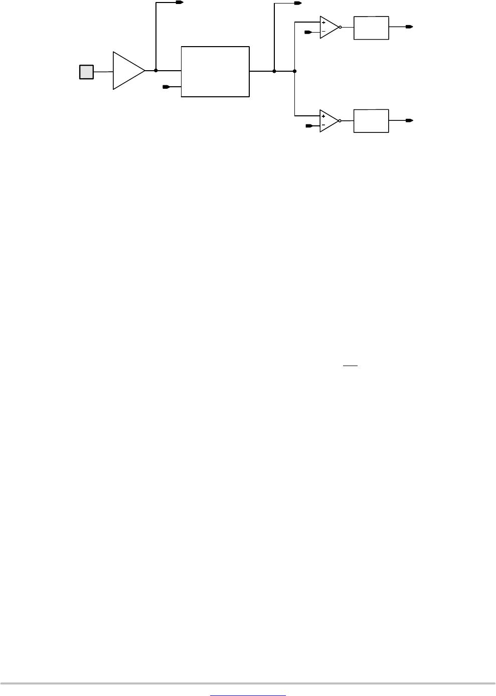
Brown−Out Detection (Versions [C**] and [D**])
For an application w/o Vaux (using the Drain) and using
Brown−out options ([C**] and [D**]) the Brown−out
feature will use the High and Low Brown−out levels.
Brown−out options ([C**] and [D**]) must not be used
on an application using Vaux as these options are not
designed to work in this case.
By default, the Brown−out flag is set High (BONOK=1),
meaning that V
in
,sensed thru CSZCD pin and V
sns
(V
sns
is
a low−pass filtered scaled down V
in
) internal signal (see
Figure 1), when higher than internal reference voltage
V
BOH
will set the brown−out flag to zero (BONOK=0) and
allow the controller to start. After BONOK is set to zero, and
switching activity starts, the V
in
continues to be sensed thru
CSZCD pin and when V
sns
falls under Brown−out internal
reference voltage V
BOL
for 50 ms, BONOK flag will be set
to 1. After BONOK flag will be set to 1, drive is not disabled,
instead, a 30 mA current source is applied to VCTRL pin to
gradually reduce V
ctrl
. As a result, the circuit only stops
pulsing when the STATICOVP function is activated (that is
when V
ctrl
reaches the SKIP detection threshold). At that
moment, the circuit stops switching. This method limits any
risk of false triggering.
For an application w/Vaux (not using the Drain),
Brown−out options ([C**] and [D**]) are not be allowed
and the UVP will act like a brown−in. The reason is that
before controller starts switching, the V
out
voltage is equal
to V
mains,rms
and sensed by FB pin and compared to UVP
high internal reference voltage V
UVPH
.
The input of the PFC stage has some impedance that leads
to some sag of the input voltage when the input current is
large. If the PFC stage suddenly stops while a high current
is drawn from the mains, the abrupt decay of the current may
make the input voltage rise and the circuit detect a correct
line level. Instead, the gradual decrease of V
control
avoids a
line current discontinuity and limits the risk of false
triggering.
V
sns
internal voltage is also used to sense the line for
feed−forward. A similar method is used:
• The V
sns
internal pin voltage is compared to a 1.801 V
reference.
• If V
sns
exceeds 1.801 V, the circuit detects a high−line
condition and the loop gain is divided by three (the
internal PWM ramp slope is three times steeper)
• Once this occurs, if V
sns
remains below 1.392 V for
25 ms, the circuit detects a low−line situation (500 mV
hysteresis).
At startup, the circuit is in High−line state (“LLINE” Low”)
and then V
sns
will be used to determine the High−Line or
Low−Line state.
The line range detection circuit allows more optimal loop
gain control for universal (wide input mains) applications.