PXAC201602FC-V1-R0

All published data at T
CASE
= 25°C unless otherwise indicated
ESD: Electrostatic discharge sensitive device—observe handling precautions!
4600 Silicon Drive | Durham, NC 27703 | www.wolfspeed.comRev. 05, 2018-07-02
PXAC201602FC
Package H-37248-4
Thermally-Enhanced High Power RF LDMOS FET
140 W, 28 V, 1880 – 1920 MHz, 2010 – 2025 MHz
Description
The PXAC201602FC is a 140-watt LDMOS FET for use in multi-
standard cellular power amplifier applications in the 1880 to 1920
MHz and 2010 to 2025 MHz frequency bands. It features input and
output matching, and a thermally-enhanced package with earless
flange. Manufactured with Wolfspeed's advanced LDMOS process, this
device provides excellent thermal performance and superior reliability.
Features
• Asymmetric Doherty design
- Main: 55 W Typ (P
1dB
)
- Peak: 85 W Typ (P
1dB
)
• Broadband internal matching
• Pulsed CW performance, 1960 MHz, 28 V
- Output power at P
1dB
= 100 W
- Gain = 18 dB
- Efficiency = 55%
• Capable of handling 10:1 VSWR @ 28 V, 140 W
(CW) output power
• Integrated ESD protection
• Human Body Model Class 1C (per JESD22-A114)
• Low thermal resistance
• Pb-free and RoHS compliant
• Can be operated with I
DQ
of up to 700 mA
(not to exceed maximum ratings limits)
RF Specifications
Single-carrier WCDMA Characteristics (tested in Wolfspeed Doherty test fixture)
V
DD
= 28 V, V
GS(PEAK)
= 1.4 V, I
DQ
= 360 mA, P
OUT
= 22.5 W average, ƒ = 2025 MHz, 3GPP WCDMA signal, channel band-
width = 3.84 MHz, 10 dB PAR @0.01% CCDF.
Characteristic Symbol Min Typ Max Unit
Gain G
ps
16.5 17.7 dB
Drain Efficiency
h
D
41 44 %
Adjacent Channel Power Ratio ACPR –28 –26 dBc
Output PAR @ 0.01% CCDF 1880 MHz OPAR 7.0 dB
Output PAR @ 0.01% CCDF 2025 MHz OPAR 7.8 dB
-60
-40
-20
0
20
40
60
0
4
8
12
16
20
24
25 30 35 40 45 50
Efficiency (%)
Gain (dB), Peak/Average Ratio
Average Output Power (dBm)
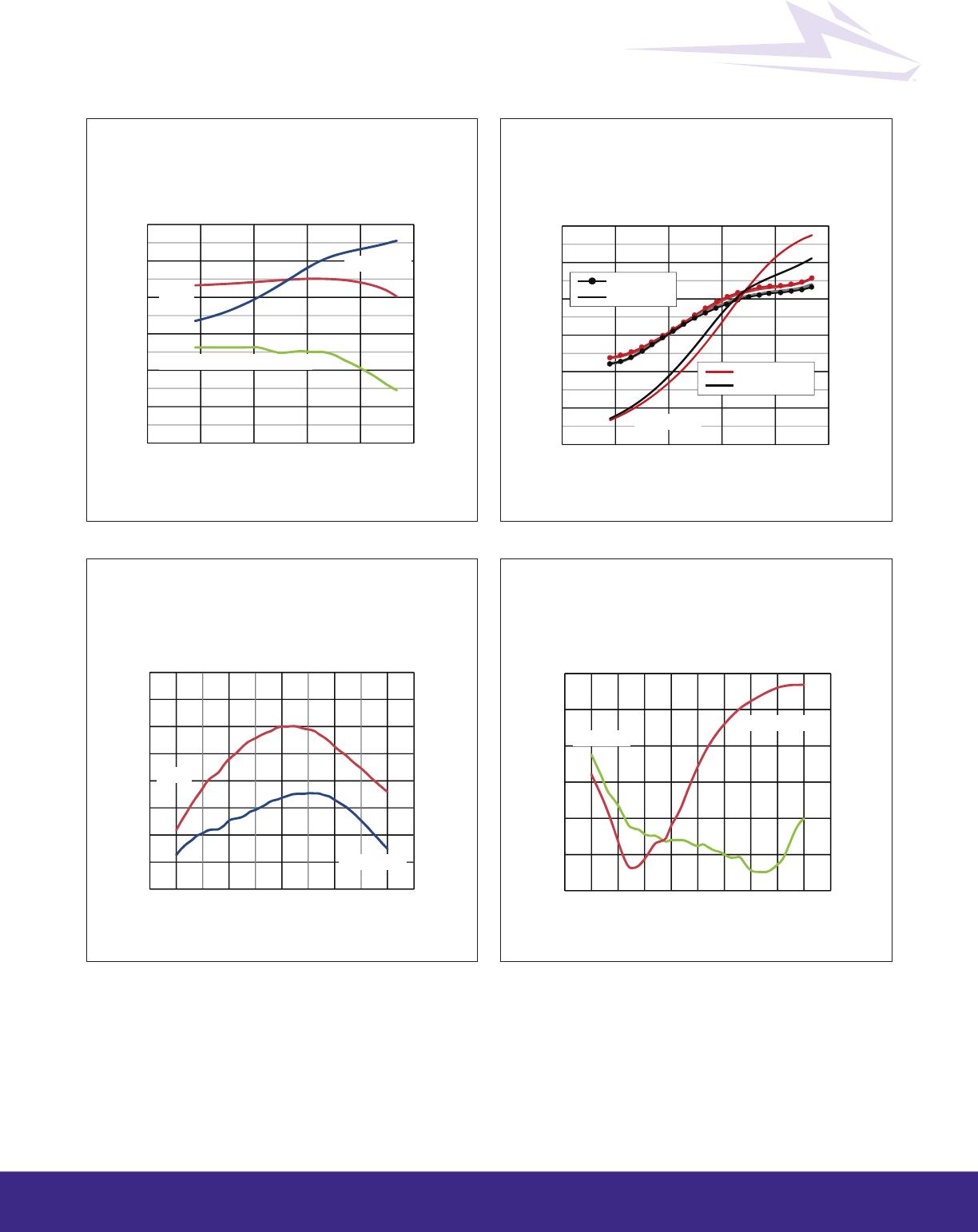
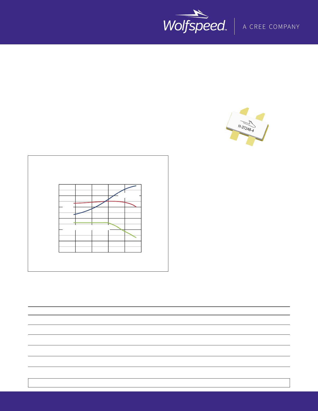
Single-carrier WCDMA Drive-up
V
DD
= 28 V, I
DQ
= 360 mA, ƒ = 1880 MHz
3GPP WCDMA signal:
10 dB PAR, 3.84 MHz BW
Gain
Efficiency
PAR @ 0.01% CCDF
c201602fc-gr1a
PXAC201602FC
4600 Silicon Drive | Durham, NC 27703 | www.wolfspeed.comRev. 05, 2018-07-02
2
PXAC201602FC
DC Characteristics
Characteristic Conditions Symbol Min Typ Max Unit
Drain-source Breakdown Voltage V
GS
= 0 V, I
DS
= 10 mA V
(BR)DSS
65 V
Drain Leakage Current V
DS
= 28 V, V
GS
= 0 V I
DSS
1.0 µA
V
DS
= 63 V, V
GS
= 0 V I
DSS
10.0 µA
Gate Leakage Current V
GS
= 10 V, V
DS
= 0 V I
GSS
1.0 µA
On-state Resistance (main) V
GS
= 10 V, V
DS
= 0.1 V R
DS(on)
0.175 W
(peak) V
GS
= 10 V, V
DS
= 0.1 V R
DS(on)
0.175 W
Operating Gate Voltage (main) V
DS
= 28 V, I
DQ
= 360 mA V
GS
2.5 2.71 2.8 V
(peak) V
DS
= 1.2 V, I
DQ
= 0 A V
GS
0.9 1.2 1.5 V
Maximum Ratings
Parameter Symbol Value Unit
Drain-source Voltage V
DSS
65 V
Gate-source Voltage V
GS
–6 to +10 V
Operating Voltage V
DD
0 to +32 V
Junction Temperature T
J
225 °C
Storage Temperature Range T
STG
–65 to +150 °C
Thermal Resistance (Doherty, T
CASE
= 70°C, 100 W CW) R
q
JC
0.48 °C/W
Ordering Information
Type and Version Order Code Package Description Shipping
PXAC201602FC V1 R0 PXAC201602FC-V1-R0 H-37248-4, ceramic open-cavity, earless Tape & Reel, 50 pcs
PXAC201602FC V1 R250 PXAC201602FC-V1-R250 H-37248-4, ceramic open-cavity, earless Tape & Reel, 250 pcs
4600 Silicon Drive | Durham, NC 27703 | www.wolfspeed.comRev. 05, 2018-07-02
3
PXAC201602FC
Typical Performance (data taken in a reference test fixture)
0
10
20
30
40
50
60
-70
-60
-50
-40
-30
-20
-10
25 30 35 40 45 50
Drain Efficiency(%)
ACP Up, ACP Low (dBc)
Average Output Power (dBm)
Single-carrier WCDMA Drive-up
V
DD
= 28 V, I
DQ
= 360 mA, ƒ = 1880 MHz and
2025 MHz. 3GPP WCDMA signal,
10 dB PAR, 3.84 MHz BW
Efficiency
ACP Up
ACP Low
1880 MHz
2025 MHz
c201602fc-gr2
30
40
50
60
70
12
14
16
18
20
1650 1750 1850 1950 2050 2150
Drain Efficiency (%)
Gain (dB)
Frequency (MHz)
Single-carrier WCDMA Broadband
Performance
V
DD
= 28 V, I
DQ
= 360 mA, P
OUT
= 43.5 dBm,
3GPP WCDMA signal,
10 dB PAR
Efficienc
y
Gain
c201602fc-gr3
-35
-30
-25
-20
-15
-10
-5
-30
-25
-20
-15
1650 1750 1850 1950 2050 2150
Return Loss (dB)
ACP Up (dBc)
Frequency (MHz)
Single-carrier WCDMA Broadband
Performance
V
DD
= 28 V, I
DQ
= 360 mA, P
OUT
= 43.5 dBm,
3GPP WCDMA signal,
10 dB PAR
Return Loss
A
CP Up
c201602fc-gr4
-60
-40
-20
0
20
40
60
0
4
8
12
16
20
24
25 30 35 40 45 50
Efficiency (%)
Gain (dB), Peak/Average Ratio
Average Output Power (dBm)
Single-carrier WCDMA Drive-up
V
DD
= 28 V, I
DQ
= 360 mA, ƒ = 2025 MHz
3GPP WCDMA signal:
10 dB PAR, 3.84 MHz BW
Gain
Efficiency
PAR @ 0.01% CCDF
c201602fc-gr1b

PXAC201602FC-V1-R0

Mfr. #:
Manufacturer:
N/A
Description:
RF MOSFET Transistors RF LDMOS FET
Lifecycle:
New from this manufacturer.
Delivery:
DHL FedEx Ups TNT EMS
Payment:
T/T Paypal Visa MoneyGram Western Union

Products related to this Datasheet