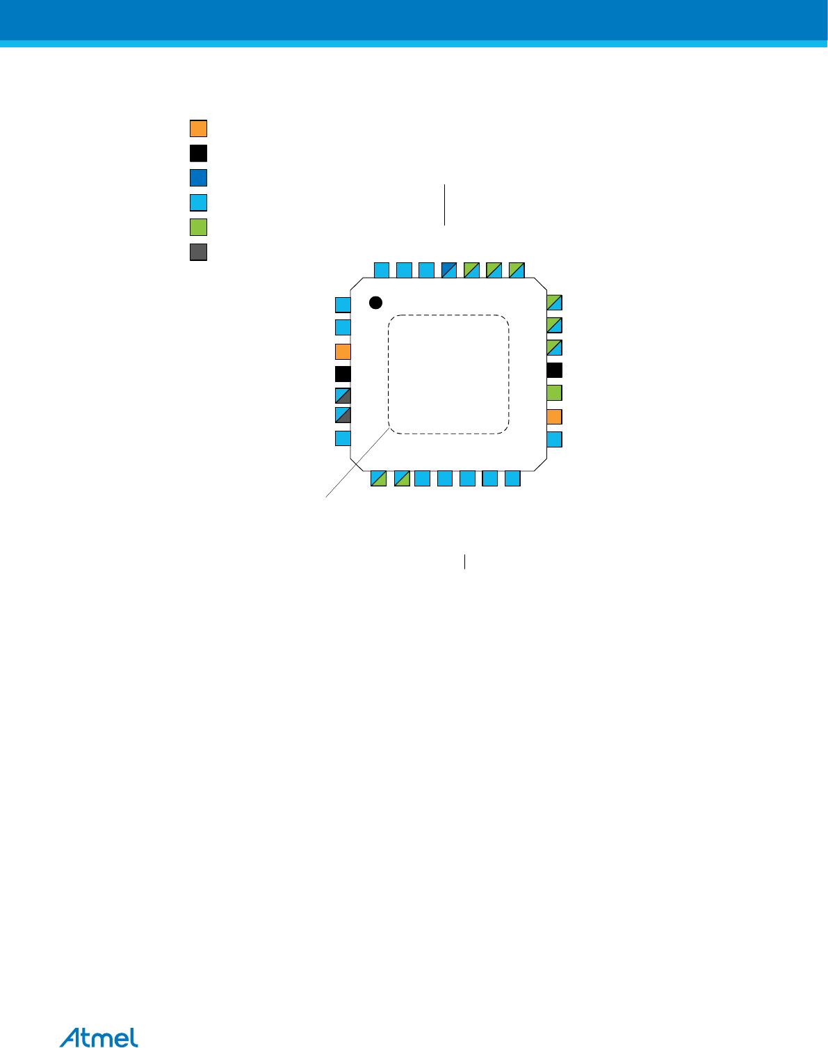
Figure 5-4. 32-pin MLF Top View
1
2
3
4
32
31
30
29
28
27
26
5
6
7
8
24
23
22
21
20
19
18
17
25
9
10
11
12
13
14
15
16
PD2 (INT0/PCINT18)
PD1 (TXD/PCINT17)
PD0 (RXD/PCINT16)
PC6 (RESET/PCINT14)
PC5 (ADC5/SCL/PCINT13)
PC4 (ADC4/SDA/PCINT12)
PC3 (ADC3/PCINT11)
PC2 (ADC2/PCINT10)
PC1 (ADC1/PCINT9)
PC0 (ADC0/PCINT8)
ADC7
GND
AREF
ADC6
AVCC
PB5 (SCK/PCINT5)
(PCINT21/OC0B/T1) PD5
(PCINT22/OC0A/AIN0) PD6
(PCINT23/AIN1) PD7
(PCINT0/CLKO/ICP1) PB0
(PCINT1/OC1A) PB1
(PCINT2/SS/OC1B) PB2
(PCINT3/OC2A/MOSI) PB3
(PCINT4/MISO) PB4
(PCINT19/OC2B/INT1) PD3
(PCINT20/XCK/T0) PD4
GND
VCC
GND
VCC
(PCINT6/XTAL1/TOSC1) PB6
(PCINT7/XTAL2/TOSC2) PB7
Bottom pad should be
soldered to ground
Power
Ground
Programming/debug
Digital
Analog
Crystal/CLK
5.2. Pin Descriptions
5.2.1. VCC
Digital supply voltage.
5.2.2. GND
Ground.
5.2.3. Port B (PB[7:0]) XTAL1/XTAL2/TOSC1/TOSC2
Port B is an 8-bit bi-directional I/O port with internal pull-up resistors (selected for each bit). The Port B
output buffers have symmetrical drive characteristics with both high sink and source capability. As inputs,
Port B pins that are externally pulled low will source current if the pull-up resistors are activated. The Port
B pins are tri-stated when a reset condition becomes active, even if the clock is not running.
Depending on the clock selection fuse settings, PB6 can be used as input to the inverting Oscillator
amplifier and input to the internal clock operating circuit.
Atmel ATmega328/P [DATASHEET]
Atmel-42735B-328/P_Datasheet_Summary-11/2016
12