NCN5150
www.onsemi.com
4
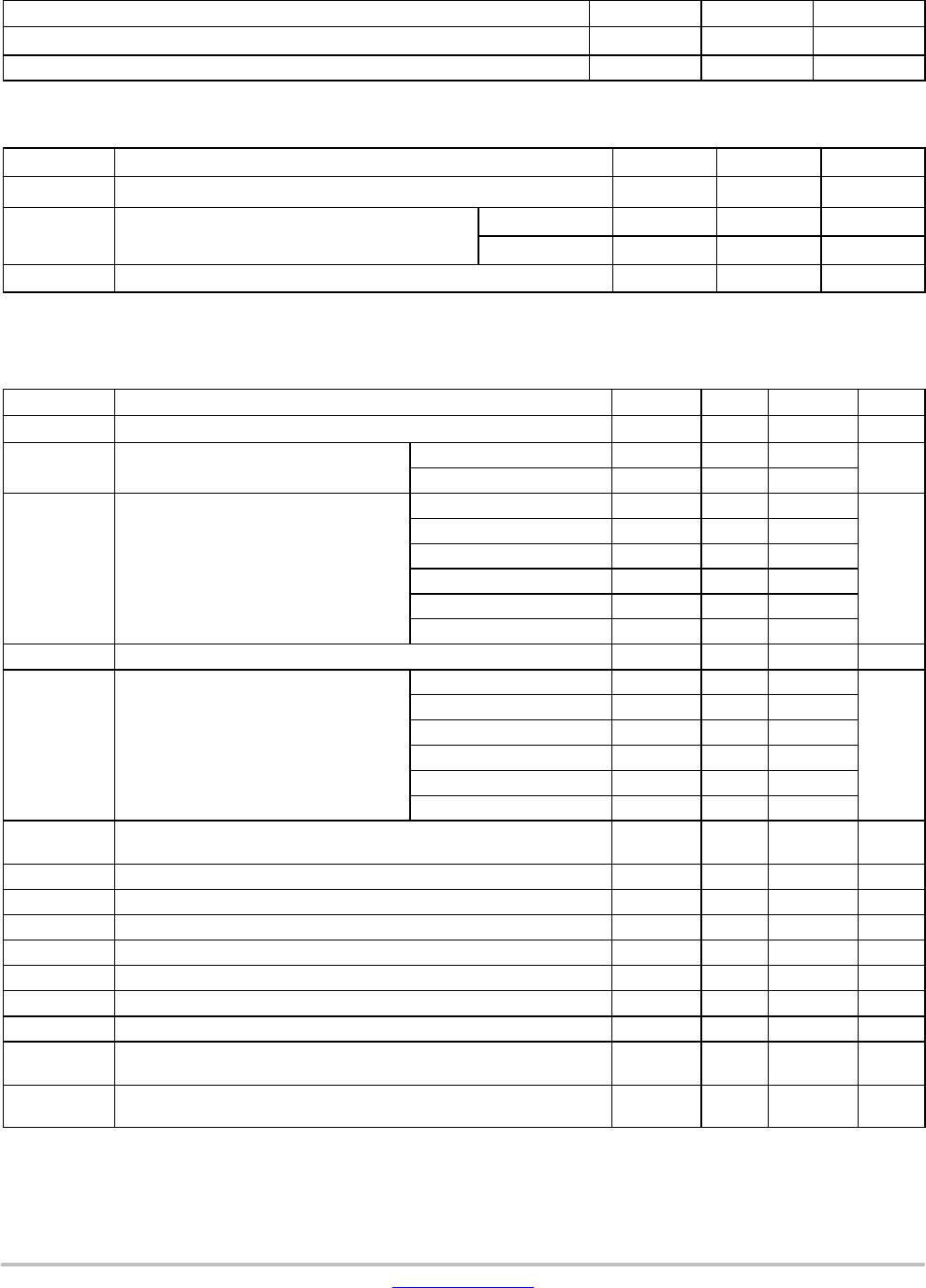
Table 3. THERMAL CHARACTERISTICS
Rating Symbol Typical Value Unit
Thermal Characteristics, SOIC−16 − Thermal Resistance, Junction-to-Air
R
θJA
125 °C/W
Thermal Characteristics, QFN−20 − Thermal Resistance, Junction-to-Air
R
θJA
42 °C/W
NOTE: R
q
JA
obtained with 1S0P (SOIC) or 2S2P (QFN) test boards according to JEDEC JESD51 standard.
Table 4. RECOMMENDED OPERATING CONDITIONS (Notes 2 and 3)
Symbol
Parameter Min Max Unit
T
A
Ambient Temperature −40 +85 °C
V
BUS
Bus Voltage (|V
BUSL1
−V
BUS2
|)
1−2 Unit Loads 9.2 42 V
3−6 Unit Loads 9.7 42 V
V
IO
VIO Pin Voltage (Note 4) 2.5 3.8 V
2. Refer to ELECTRICAL CHARACTERISTICS and APPLICATION INFORMATION for Safe Operating Area.
3. All voltages are referenced to GND.
4. V
STC
must be at least 1V higher than V
IO
for proper operation.
Table 5. ELECTRICAL CHARACTERISTICS (Note 5)
Symbol Parameter Min Typ Max Unit
DV
BR
Voltage drop over bus rectifier (V
BUS
− V
B
) (R
IDD
(Note 6) = 4.02 kW)
− − 1.25 V
DV
CS
Voltage drop over CS1
(V
B
− V
STC
)
R
IDD
(Note 6) ≥ 13 kW
1.30 − −
V
R
IDD
(Note 6) ≤ 4.02 kW
1.70 − −
I
BUS
Total Current Drawn from the Bus, Mark
State
R
IDD
(Note 6) = 30 kW
− 1.32 1.50
mA
R
IDD
(Note 6) = 13 kW
− 2.71 3.00
R
IDD
(Note 6, 7) = 8.45 kW
− 4.10 4.50
R
IDD
(Note 6, 7) = 6.19 kW
− 5.50 6.00
R
IDD
(Note 6, 7) = 4.87 kW
− 6.80 7.50
R
IDD
(Note 6, 7) = 4.02 kW
− 8.22 9.00
DI
BUS
Bus Current Stability (over DV
BUS
= 10 V, RX/RXI = mark)
− 0.2 2 %
I
STC
Idle Current Available for the Application
to Draw from STC and V
DD
(Including
Current Drawn from IO Pins)
R
IDD
(Note 6) = 30 kW
0.88 1.05 1.20
mA
R
IDD
(Note 6) = 13 kW
2.10 2.35 2.60
R
IDD
(Note 6, 7) = 8.45 kW
3.10 3.60 4.00
R
IDD
(Note 6, 7) = 6.19 kW
4.20 4.80 5.40
R
IDD
(Note 6, 7) = 4.87 kW
5.30 6.10 6.90
R
IDD
(Note 6, 7) = 4.02 kW
6.50 7.45 8.40
DI
STC, space
Additional Current Available for the Application when Transmitting a
Space
− 200 −
mA
I
CC
Internal Supply Current (R
IDD
(Note 6) = 13 kW, RX/RXI = mark)
− 359 500
mA
I
IO
Current Drawn by the V
IO
Pin −0.5 − 0.5
mA
V
STC, clamp
Clamp Voltage on Pin STC (I
DD
< I
STC
) 6.0 6.5 7.0 V
V
B, PFb
Threshold Voltage on V
B
to Trigger PFb (Note 8) V
STC
+ 0.3 − V
STC
+ 0.8 V
V
PFb, OH
PFb Voltage High (I
PFb
= −100 mA)
V
IO
− 0.6 − V
IO
V
V
PFb, OL
PFb Voltage Low (Note 9) (I
PFb
= 50 mA)
0 − 0.6 V
V
RIDD
Voltage on RIDD Pin 1.15 1.20 1.25 V
V
VS, OH
Voltage on VS during High State
(V
STC
> V
STC, VDD ON
, I
VS
= −5 mA)
V
STC
− 0.4 − V
STC
V
R
VS, PD
Pull-down Resistor on VS during Low State
(V
DD
> 2 V, V
STC
> V
S
)
50 100 150
kW
5. All voltages are referenced to GND.
6. Resistor with 1% accuracy.
7. Only possible in NQFP variant.
8. PFb comparator has a 70 mV hysteresis.
9. PFb pin is pulled down with an on-chip resistor of typically 2 MW.