AQY410SX

–1–
ASCTB140E 201404-T
TYPES
* Indicate the peak AC and DC values.
Note: For space reasons, the three initial letters of the part number “AQY”, the surface mount terminal shape indicator “S” and the packing style indicator “X” or “Z” are not
marked on the device. (Ex. the label for product number AQY412SX is 412)
RATING
1. Absolute maximum ratings (Ambient temperature: 25°C 77°F)
Normally closed
SOP4-pin type
of 60V/350V/400V
load voltage
GU SOP 1 Form B
(AQY41S)
Output rating*
Package
Part No. Packing quantity
Load
voltage
Load
current
Tube packing style
Tape and reel packing style
Tube Tape and reel
Picked from the
1/2-pin side
Picked from the
3/4-pin side
AC/DC
dual use
60V 500mA
SOP4-pin
AQY412S AQY412SX AQY412SZ
1 tube contains:
100 pcs.
1 batch contains:
2,000 pcs.
1,000 pcs.350V 120mA AQY410S AQY410SX AQY410SZ
400V 100mA AQY414S AQY414SX AQY414SZ
Item Symbol AQY412S AQY410S AQY414S Remarks
Input
LED forward current I
F 50 mA
LED reverse voltage VR 5 V
Peak forward current IFP 1 A f = 100 Hz, Duty factor = 0.1%
Power dissipation Pin 75 mW
Output
Load voltage (peak AC) VL 60 V 350 V 400 V
Continuous load current IL 0.5 A 0.12 A 0.1 A Peak AC, DC
Peak load current Ipeak 1.5 A 0.3 A 0.24 A 100ms (1 shot), VL = DC
Power dissipation Pout 300 mW
Total power dissipation PT 350 mW
I/O isolation voltage Viso 1,500 V AC
Temperture
limits
Operating T
opr –40°C to +85°C –40°F to +185°F Non-condensing at low temperatures
Storage Tstg –40°C to +100°C –40°F to +212°F
(AQY412S)
(AQY410S, 414S)
VDE
mm inch
FEATURES
1. Small SOP4-pin package
The device comes in a super-miniature
SO package 4-pin type measuring
(W) 4.3×(L) 4.4×(H) 2.1 mm (W) .169×(L)
.173×(H) .083 inch
2. Low on-resistance
The AQ4 series (normally closed type)
has a low on-resistance.
This has been achieved thanks to the
built-in MOSFET processed by our
proprietary method, DSD (Double-
diffused and Selective Doping) method.
3. Controls low-level analog signals
PhotoMOS feature extremely low closed-
circuit offset voltage to enable control of
low-level analog signals without
distortion.
4. Low-level off-state leakage current
of max. 1 μA
TYPICAL APPLICATIONS
• Power supply
• Measuring instruments
• Security equipment
• Telephone equipment
• Sensing equipment
4.4
2.1
4.3
.173
.083
.169
1
2
4
3
RoHS compliant
Source electrode
N
N
+
N
+
N
+
P
+
N
+
N
+
P
+
Gate electrode
Passivation membrane
Cross section of the normally-closed type of
power MOS
Intermediate
insulating
membrane
Gate
oxidation
membrane
Drain
electrode
GU SOP 1 Form B (AQY41S)
–2–
ASCTB140E 201404-T
2. Electrical characteristics (Ambient temperature: 25°C 77°F)
*Operate/Reverse time
RECOMMENDED OPERATING CONDITIONS
Please obey the following conditions to ensure proper device operation and resetting.
These products are not designed for automotive use.
If you are considering to use these products for automotive applications, please contact your local Panasonic Corporation
technical representative.
REFERENCE DATA
Item Symbol AQY412S AQY410S AQY414S Remarks
Input
LED operate (OFF) current
Typical
IFoff
0.9 mA
IL = Max.
Maximum 3 mA
LED reverse (ON) current
Minimum
IFon
0.4 mA
IL = Max.
Typical 0.85 mA
LED dropout voltage
Typical
VF
1.25 V (1.14 V at IF = 5 mA)
IF = 50 mA
Maximum 1.5 V
Output
On resistance
Typical
R
on
1 Ω 18 Ω 26 Ω
I
F = 0 mA
I
L = Max.
Within 1 s on time
Maximum 2.5 Ω 25 Ω 35 Ω
Off state leakage current Maximum I
Leak 1 μA
I
F = 5 mA
V
L = Max.
Transfer
characteristics
Operate (OFF) time*
Typical
T
off
0.9 ms 0.52 ms 0.47 ms
I
F = 0 mA 5 mA
I
L = Max.
Maximum 3 ms 1 ms
Reverse (ON) time*
Typical
T
on
0.21 ms 0.23 ms 0.28 ms
I
F = 5 mA 0 mA
I
L = Max.
Maximum 1 ms
I/O capacitance
Typical
C
iso
0.8 pF
f = 1 MHz
V
B = 0 V
Maximum 1.5 pF
Initial I/O isolation resistance Minimum R
iso 1,000 MΩ 500 V DC
Item Symbol Recommended value Unit
Input LED current I
F 5mA
Toff
Input
Output
10%
90%
Ton
1. Load current vs. ambient temperature
characteristics
Allowable ambient temperature:
–40°C to +85°C
–40°F to +185°F
2. On resistance vs. ambient temperature
characteristics
Measured portion: between terminals 3 and 4;
LED current: 0 mA;
Continuous load current: Max.(DC)
3. Operate (OFF) time vs. ambient temperature
characteristics
LED current: 5 mA; Load voltage: Max.(DC);
Continuous load current: Max.(DC)
Load current, mA
-40 100
Ambient temperature, °C
600
500
400
300
200
100
0
700
0-20 20 40 60
80 85
100
AQY410S
AQY414S
AQY412S
On resistance, Ω
0204060
80 85
100
Ambient temperature, °C
30
15
10
25
20
5
0
-40 -20
AQY410S
AQY414S
AQY412S
Operate (OFF) time, ms
0-40 -20 20 40 60
80 85
100
Ambient temperature, °C
2
1.5
1
0.5
0
AQY410S
AQY414S
AQY412S
GU SOP 1 Form B (AQY41S)
–3–
ASCTB140E 201404-T
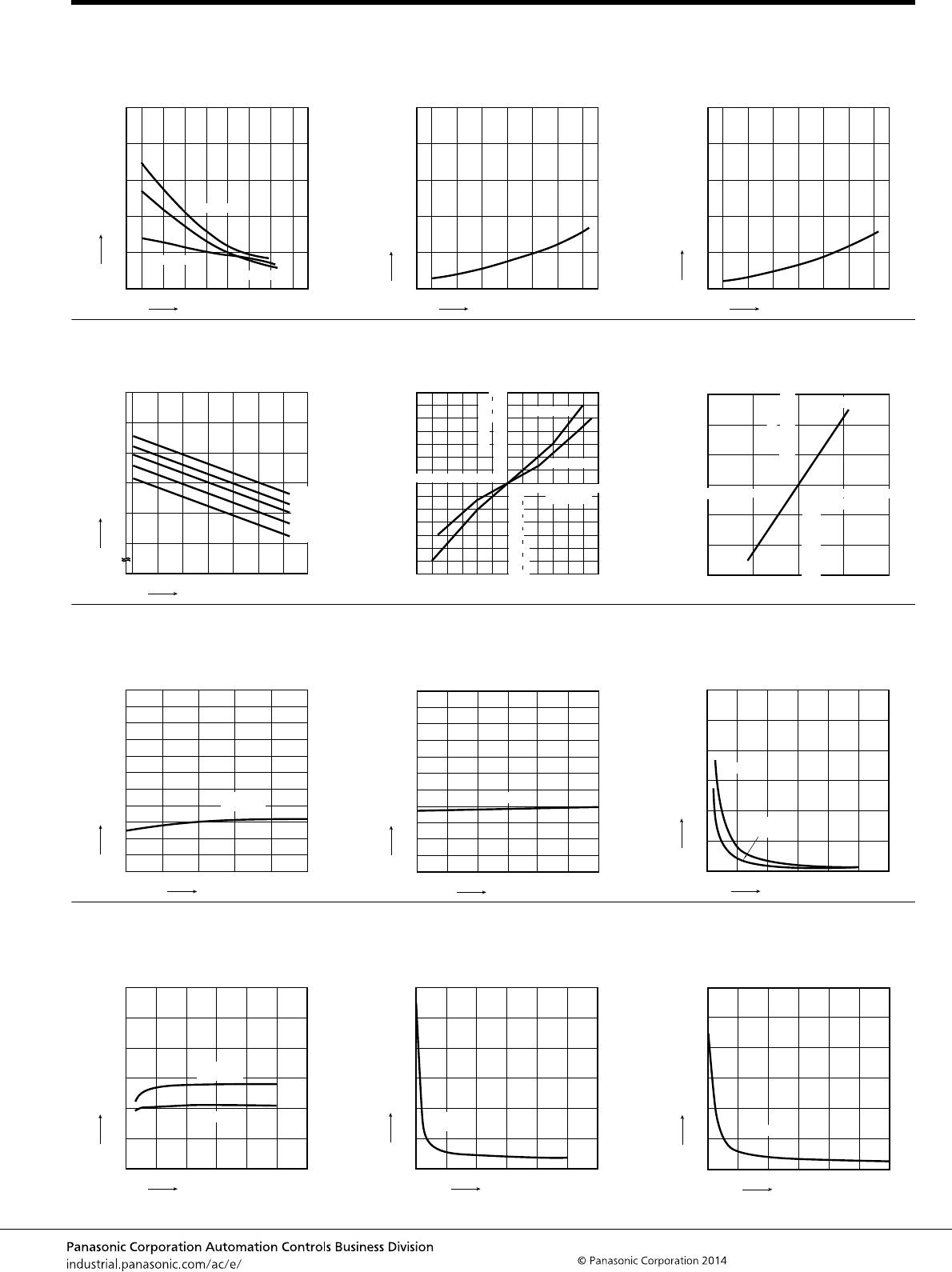
4. Reverse (ON) time vs. ambient temperature
characteristics
LED current: 5 mA; Load voltage: Max.(DC);
Continuous load current: Max.(DC)
5. LED operate (OFF) current vs. ambient
temperature characteristics
Sample: All types;
Load voltage: Max.(DC);
Continuous load current: Max.(DC)
6. LED reverse (ON) current vs. ambient
temperature characteristics
Sample: All types;
Load voltage: Max.(DC);
Continuous load current: Max.(DC)
Reverse (ON) time, ms
0-20-40 20 40 60 100
80 85
Ambient temperature, °C
1.0
0.8
0.6
0.4
0.2
0
AQY410S
AQY414S
AQY412S
0–40 –20 20 40 60
80 85
5
4
3
2
1
0
Ambient temperature, °C
LED operate (OFF) current, mA
0204060
80 85
5
4
3
2
1
0
-40 -20
Ambient temperature, °C
LED reverse (ON) current, mA
7. LED dropout voltage vs. ambient
temperature characteristics
Sample: All types;
LED current: 5 to 50 mA
8-(1). Current vs. voltage characteristics of
output at MOS portion
Measured portion: between terminals 3 and 4;
Ambient temperature: 25°C 77°F
8-(2). Current vs. voltage characteristics of
output at MOS portion
Measured portion: between terminals 3 and 4;
Ambient temperature: 25°C 77°F
0–40 –20 20 40 60
80 85
Ambient temperature, °C
LED dropout voltage, V
1.5
1.4
1.3
1.2
1.1
1.0
0
50mA
30mA
20mA
10mA
5mA
AQY410S
AQY414S
1.5 2.50.5 1 2 3
-20
-40
-60
-80
-100
-120
-140
140
120
100
80
60
40
20
-3 -2 -1-2.5 -1.5 -0.5
Current, mA
Voltage, V
0.2
0.4
0.6
-0.2
-0.4
-0.6
-1
-0.5
0.5 1
Voltage, V
Current, A
AQY412S
9-(1). Off state leakage current vs. load voltage
characteristics
Measured portion: between terminals 3 and 4;
LED current: 5 mA; Ambient temperature: 25°C 77°F
9-(2). Off state leakage current vs. load voltage
characteristics
Measured portion: between terminals 3 and 4;
LED current: 5 mA; Ambient temperature: 25°C 77°F
10. Operate (OFF) time vs. LED forward
current characteristics
Measured portion: between terminals 3 and 4;
Load voltage: Max.(DC); Continuous load current:
Max.(DC); Ambient temperature: 25°C 77°F
Off state leakage current, A
2006040 80 100
Load voltage, V
10
–3
10
–6
10
–9
10
–12
AQY414S
AQY410S
2010 30 5006040
Load voltage, V
10
–3
10
–5
10
–9
10
–7
10
–11
10
–13
AQY412S
Off state leakage current, A
Operate (OFF) time, ms
100 2030405060
3.0
2.5
2.0
1.5
1.0
0.5
0
LED forward current, mA
AQY412S
AQY410S
AQY414S
11. Reverse (ON) time vs. LED forward current
characteristics
Measured portion: between terminals 3 and 4;
Load voltage: Max.(DC); Continuous load current:
Max.(DC); Ambient temperature: 25°C 77°F
12-(1). Output capacitance vs. applied voltage
characteristics
Measured portion: between terminals 3 and 4;
Frequency: 1 MHz;
LED current: 5 mA; Ambient temperature: 25°C 77°F
12-(2). Output capacitance vs. applied voltage
characteristics
Measured portion: between terminals 3 and 4;
Frequency: 1 MHz;
LED current: 5 mA; Ambient temperature: 25°C 77°F
Reverse (ON) time, ms
LED forward current, mA
10 20 30 40 50 60100 2030405060
0.6
0.5
0.4
0.3
0.2
0.1
0
AQY412S
AQY414S
AQY410S
Output capacitance, pF
100 2030405060
120
100
80
60
40
20
0
Applied voltage, V
AQY414S
AQY410S
100 2030405060
600
500
400
300
200
100
0
Applied voltage, V
AQY412S
Output capacitance, pF

AQY410SX

Mfr. #:
Manufacturer:
Panasonic
Description:
Solid State Relays - PCB Mount 350v 130mA SOP Form B Norm-Clsd
Lifecycle:
New from this manufacturer.
Delivery:
DHL FedEx Ups TNT EMS
Payment:
T/T Paypal Visa MoneyGram Western Union

Products related to this Datasheet