VOL617A
www.vishay.com
Vishay Semiconductors
Rev. 2.0, 13-Oct-15
1
Document Number: 82424
For technical questions, contact: optocoupleranswers@vishay.com
THIS DOCUMENT IS SUBJECT TO CHANGE WITHOUT NOTICE. THE PRODUCTS DESCRIBED HEREIN AND THIS DOCUMENT
ARE SUBJECT TO SPECIFIC DISCLAIMERS, SET FORTH AT www.vishay.com/doc?91000
Optocoupler, Phototransistor Output, 4 Pin LSOP,
Long Creepage Mini-Flat Package
DESCRIPTION
The VOL617A has a GaAs infrared emitting diode emitter,
which is optically coupled to a silicon planar phototransistor
detector, and is incorporated in a 4 pin LSOP wide body
package.
It features a high current transfer ratio, low coupling
capacitance, and high isolation voltage.
The coupling device is designed for signal transmission
between two electrically separated circuits.
FEATURES
• Low profile package
• High collector emitter voltage, V
CEO
= 80 V
• Isolation test voltage, 5000 V
RMS
• Isolation voltage V
IORM
= 1050 V
peak
• Low coupling capacitance
• High common mode transient immunity
• Material categorization:
for definitions of compliance please see
www.vishay.com/doc?99912
APPLICATIONS
• Telecom
• Industrial controls
• Battery powered equipment
• Office machines
• Programmable controllers
AGENCY APPROVALS
(All parts are certified under base model VOL617A)
• UL1577, file no. E76222
• cUL CSA 22.2 bulletin 5A, double protection
• DIN EN 60747-5-5 (VDE 0884-5), available with option 1
• BSI: EN 60065:2002, EN 60950-1:2006
• FIMKO EN60950-1
• CQC: GB8898-2011, GB4943.1-2011
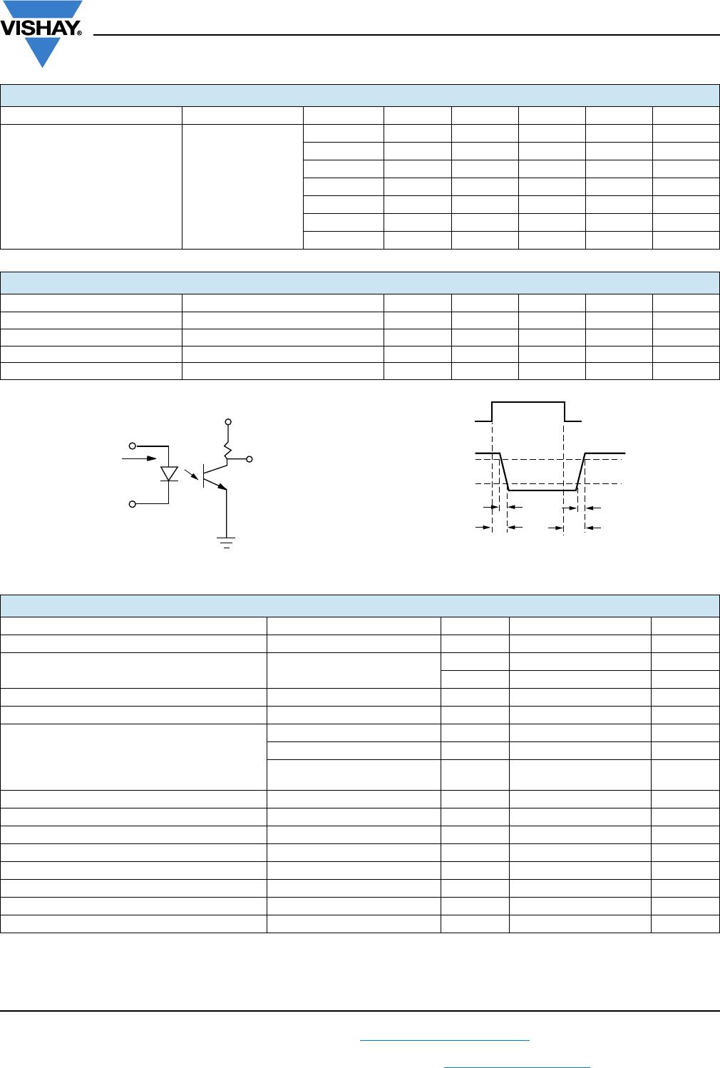
E
CA
C
1
2
4
3
ORDERING INFORMATION
VOL617A-#X001 T
PART NUMBER CTR
BIN
PACKAGE OPTION TAPE
AND
REEL
AGENCY CERTIFIED/
PACKAGE
CTR (%)
5 mA
UL, cUL, BSI,
FIMKO, CQC
50 to 600 40 to 80 63 to 125 100 to 200 160 to 320 80 to 160 130 to 260
4 pin LSOP, mini-flat,
long creepage
VOL617AT VOL617A-1T VOL617A-2T VOL617A-3T VOL617A-4T - -
UL, cUL, BSI, FIMKO,
CQC, VDE (option 1)
50 to 600 40 to 80 63 to 125 100 to 200 160 to 320 80 to 160 130 to 260
4 pin LSOP, mini-flat,
long creepage
VOL617A-
X001T
VOL617A-
1X001T
VOL617A-
2X001T
VOL617A-
3X001T
VOL617A-
4X001T
VOL617A-
7X001T
VOL617A-
8X001T