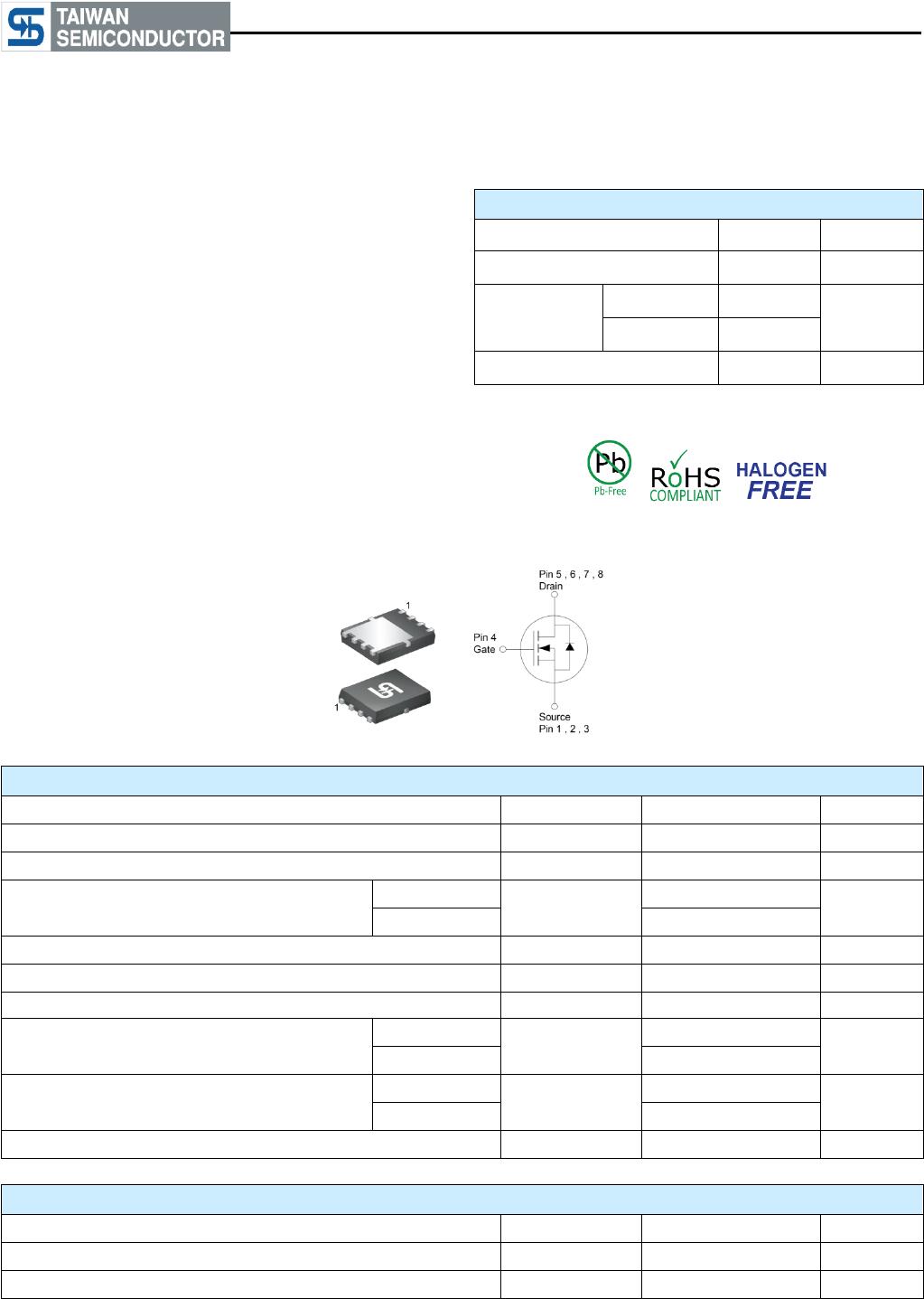
TSM280NB06LCR RLG

TSM280NB06LCR
Taiwan Semiconductor
1 Version: B1804
N-Channel Power MOSFET
60V, 28A, 28mΩ
FEATURES
Low R
DS(ON)
to minimize conductive losses
Logic level
Low gate charge for fast power switching
100% UIS and R
g
tested.
175°C Operating Junction Temperature
Compliant to RoHS directive 2011/65/EU and in
accordance to WEEE 2002/96/EC
Halogen-free according to IEC 61249-2-21
APPLICATIONS
BLDC Motor Control
Battery Power Management
DC-DC converter
Secondary Synchronous Rectification
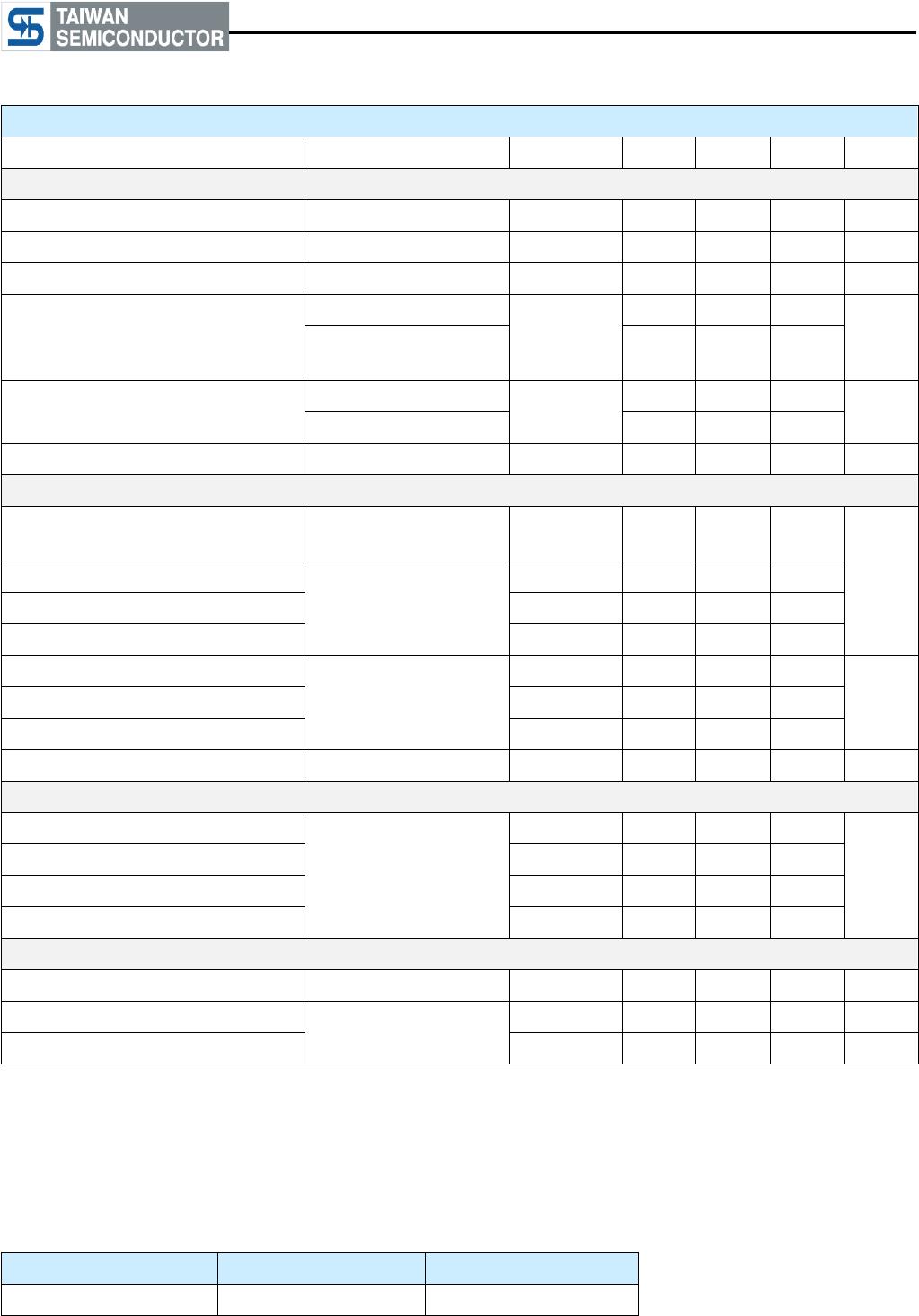
KEY PERFORMANCE PARAMETERS
PARAMETER
VALUE
UNIT
V
DS
60
V
R
DS(on)
(max)
V
GS
= 10V
28
mΩ
V
GS
= 4.5V
39
Q
g
9
nC
Note: MSL 1 (Moisture Sensitivity Level) per J-STD-020
ABSOLUTE MAXIMUM RATINGS (T
A
= 25°C unless otherwise noted)
PARAMETER
SYMBOL
LIMIT
UNIT
Drain-Source Voltage
V
DS
60
V
Gate-Source Voltage
V
GS
±20
V
Continuous Drain Current
(Note 1)
T
C
= 25°C
I
D
28
A
T
A
= 25°C
7
Pulsed Drain Current
I
DM
112
A
Single Pulse Avalanche Current
(Note 2)
I
AS
12
A
Single Pulse Avalanche Energy
(Note 2)
E
AS
22
mJ
Total Power Dissipation
T
C
= 25°C
P
D
56
W
T
C
= 125°C
19
Total Power Dissipation
T
A
= 25°C
P
D
3.1
W
T
A
= 125°C
1
Operating Junction and Storage Temperature Range
T
J
, T
STG
- 55 to +175
°C
THERMAL PERFORMANCE
PARAMETER
SYMBOL
LIMIT
UNIT
Junction to Case Thermal Resistance
R
ӨJC
2.7
°C/W
Junction to Ambient Thermal Resistance
R
ӨJA
48
°C/W
Thermal Performance Note: R
ӨJA
is the sum of the junction-to-case and case-to-ambient thermal resistances. The case-
thermal reference is defined at the solder mounting surface of the drain pins. R
ӨJA
is guaranteed by design while R
ӨCA
is
determined by the user’s board design. The R
ӨJA
limit presented here is based on mounting on a 1 in
2
pad of 2 oz copper.
TSM280NB06LCR
Taiwan Semiconductor
2 Version: B1804
ELECTRICAL SPECIFICATIONS (T
A
= 25°C unless otherwise noted)
PARAMETER
CONDITIONS
SYMBOL
MIN
TYP
MAX
UNIT
Static
Drain-Source Breakdown Voltage
V
GS
= 0V, I
D
= 250µA
BV
DSS
60
--
--
V
Gate Threshold Voltage
V
GS
= V
DS
, I
D
= 250µA
V
GS(TH)
1
2
2.5
V
Gate-Source Leakage Current
V
GS
= ±20V, V
DS
= 0V
I
GSS
--
--
±100
nA
Drain-Source Leakage Current
V
GS
= 0V, V
DS
= 60V
I
DSS
--
--
1
µA
V
GS
= 0V, V
DS
= 60V
T
J
= 125°C
--
--
100
Drain-Source On-State Resistance
(Note 3)
V
GS
= 10V, I
D
= 7A
R
DS(on)
--
24
28
mΩ
V
GS
= 4.5V, I
D
= 6A
--
32
39
Forward Transconductance
(Note 3)
V
DS
= 10V, I
D
= 7A
g
fs
--
31
--
S
Dynamic
(Note 4)
Total Gate Charge
V
GS
= 10V, V
DS
= 30V,
I
D
= 7A
Q
g
--
18
--
nC
Total Gate Charge
V
GS
= 4.5V, V
DS
= 30V,
I
D
= 6A
Q
g
--
9
--
Gate-Source Charge
Q
gs
--
3
--
Gate-Drain Charge
Q
gd
--
4
--
Input Capacitance
V
GS
= 0V, V
DS
= 30V
f = 1.0MHz
C
iss
--
969
--
pF
Output Capacitance
C
oss
--
71
--
Reverse Transfer Capacitance
C
rss
--
24
--
Gate Resistance
f = 1.0MHz
R
g
0.7
2.4
4.8
Ω
Switching
(Note 4)
Turn-On Delay Time
V
GS
= 10V, V
DS
= 30V,
I
D
= 7A, R
G
= 2Ω
t
d(on)
--
1
--
ns
Turn-On Rise Time
t
r
--
19
--
Turn-Off Delay Time
t
d(off)
--
10
--
Turn-Off Fall Time
t
f
--
18
--
Source-Drain Diode
Forward Voltage
(Note 3)
V
GS
= 0V, I
S
= 7A
V
SD
--
--
1.2
V
Reverse Recovery Time
I
S
= 7A ,
dI/dt = 100A/μs
t
rr
--
11
--
ns
Reverse Recovery Charge
Q
rr
--
5
--
nC
Notes:
1. Silicon limited current only.
2. L = 0.3mH, V
GS
= 10V, V
DD
= 30V, R
G
= 25Ω, I
AS
= 12A, Starting T
J
= 25°C
3. Pulse test: Pulse Width ≤ 300µs, duty cycle ≤ 2%.
4. Switching time is essentially independent of operating temperature.
ORDERING INFORMATION
PART NO.
PACKAGE
PACKING
TSM280NB06LCR RLG
PDFN56
2,500pcs / 13 Reel
TSM280NB06LCR
Taiwan Semiconductor
3 Version: B1804
CHARACTERISTICS CURVES
(T
A
= 25°C unless otherwise noted)
Output Characteristics
Transfer Characteristics
On-Resistance vs. Drain Current
Gate-Source Voltage vs. Gate Charge
On-Resistance vs. Junction Temperature
On-Resistance vs. Gate-Source Voltage
I
D
, Drain Current (A)
V
GS
, Gate to Source Voltage (V)
V
DS
, Drain to Source Voltage (V)
R
DS(on)
, Drain-Source On-Resistance (Ω)
I
D
, Drain Current (A)
V
GS
, Gate to Source Voltage (V)
Q
g
, Gate Charge (nC)
R
DS(on)
, Drain-Source On-Resistance
(Normalized)
T
J
, Junction Temperature (°C)
R
DS(on)
, Drain-Source On-Resistance (Ω)
V
GS
, Gate to Source Voltage (V)
I
D
, Drain Current (A)
0
2
4
6
8
10
0 5 10 15 20
V
DS
=30V
I
D
=7A
0
0.5
1
1.5
2
2.5
3
-75 -50 -25 0 25 50 75 100 125 150 175
V
GS
=10V
I
D
=7A
0
5
10
15
20
25
0 1 2 3 4 5
V
GS
=10V
V
GS
=7V
V
GS
=5V
V
GS
=4.5V
V
GS
=4V
V
GS
=3.5V
V
GS
=3V
0
0.01
0.02
0.03
0.04
0.05
0.06
0 5 10 15 20 25
V
GS
=10V
V
GS
=4.5V
0
0.02
0.04
0.06
0.08
0.1
3 4 5 6 7 8 9 10
I
D
=7A
0
5
10
15
20
25
0 1 2 3 4 5
25
-55
175

TSM280NB06LCR RLG

Mfr. #:
Manufacturer:
Taiwan Semiconductor
Description:
MOSFET 60V 28A 28mOhm N-Chan Pwr MOSFET
Lifecycle:
New from this manufacturer.
Delivery:
DHL FedEx Ups TNT EMS
Payment:
T/T Paypal Visa MoneyGram Western Union

Products related to this Datasheet