14
LTC2845
sn2845 2845fs
DTE vs DCE Operation
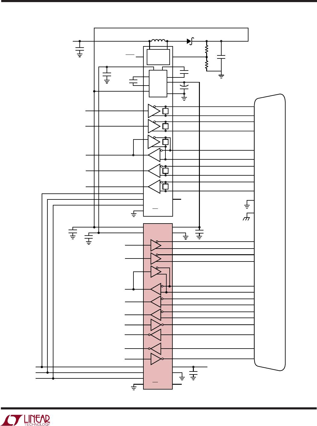
The DCE/DTE pin acts as an enable for Driver 3/Receiver␣ 1
in the LTC2846, and Driver 3/Receiver 1 in the LTC2845.
The LTC2846/LTC2845 can be configured for either DTE
or DCE operation in one of two ways: a dedicated DTE or
DCE port with a connector of appropriate gender, or a port
with one connector that can be configured for DTE or DCE
operation by rerouting the signals to the LTC2846/LTC2845
using a dedicated DTE cable or dedicated DCE cable.
A dedicated DTE port using a DB-25 male connector is
shown in Figure 23. The interface mode is selected by logic
outputs from the controller or from jumpers to either V
IN
or GND on the mode select pins. A dedicated DCE port
using a DB-25 female connector is shown in Figure 24.
A port with one DB-25 connector, can be configured for
either DTE or DCE operation is shown in Figure 25. The
configuration requires separate cables for proper signal
routing in DTE or DCE operation. For example, in DTE
mode, the TXD signal is routed to Pins 2 and 14 via Driver␣ 1
in the LTC2846. In DCE mode, Driver 1 now routes the RXD
signal to Pins 2 and 14.
Compliance Testing
The LTC2846/LTC2845 chipset has been tested by TUV
Rheinland of North America Inc. and passed the NET1,
NET2 and TBR2 requirements. Copies of the test report are
available from LTC or TUV Rheinland of North America Inc.
The title of the report is Test Report No.TBR2/050101/02
The address of TUV Rheinland of North America Inc. is:
TUV Rheinland of North America Inc.
1775, Old Highway 8 NW, Suite 107
St. Paul, MN 55112
Tel. (651) 639-0775
Fax (651) 639-0873
No-Cable Mode
The no-cable mode (M0 = M1 = M2 = D4ENB = 1, R4EN = 0)
is intended for the case when the cable is disconnected
from the connector. The bias circuitry, drivers and receiv-
ers are turned off, the driver outputs are forced into a high
impedance state, and the supply current drops to less than
700µA.
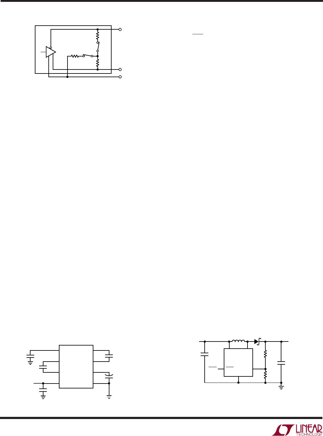
LTC2846 and LTC2847 Supplies
The LTC2846 and LTC2847 use an internal capacitive
charge pump to generate V
DD
and V
EE
as shown in Figure
21. A voltage doubler generates about 8V on V
DD
and a
voltage inverter generates about –7.5V for V
EE
. Three 1µF
surface mounted tantalum or ceramic capacitors are re-
quired for C1, C2 and C3. The V
EE
capacitor C4 should be
a minimum of 3.3µF. All capacitors are 16V and should be
placed as close as possible to the LTC2846 to reduce EMI.
The LTC2846 has an internal boost switching regulator
which generates a 5V output from the 3.3V supply as
shown in Figure 22. The 5V V
CC
supplies its internal charge
pump and transceivers as well as its companion chip. The
LTC2847 requires an external 5V supply.
Receiver Fail-Safe
All LTC2846/LTC2845 receivers feature fail-safe opera-
tion in all modes. If the receiver inputs are left floating or
shorted together by a termination resistor, the receiver
output will always be forced to a logic high.
APPLICATIONS INFORMATION
WUU
U
2845 F21
C3
1µF
C5
10µF
5V
C1
1µF
C2
1µF
C4
3.3µF
LTC2846
OR
LTC2847
V
DD
C1
+
C1
–
V
CC
C2
+
C2
–
V
EE
GND
+
Figure 21. Charge Pump Figure 22. LTC2846 Boost Switching Regulator
GND
V
IN
SW
SHDN FB
V
IN
3.3V
2845 F22
D1
L1
5.6µH
R1
13k
BOOST
SWITCHING
REGULATOR
C5
10µF
C6
10µF
R2
4.3k
V
CC
5V
480mA
C1,C2: TAIYO YUDEN X5R JMK316BJ106ML
D1: ON SEMICONDUCTOR MBR0520
L1: SUMIDA CR43-5R6
SHDN
Figure 20. V.35 Driver
V.35 DRIVER
A
B
C
51.5Ω
S2
S1
2845 F20
51.5Ω
LTC2846
124Ω