LTC3225/LTC3225-1
5
3225fb
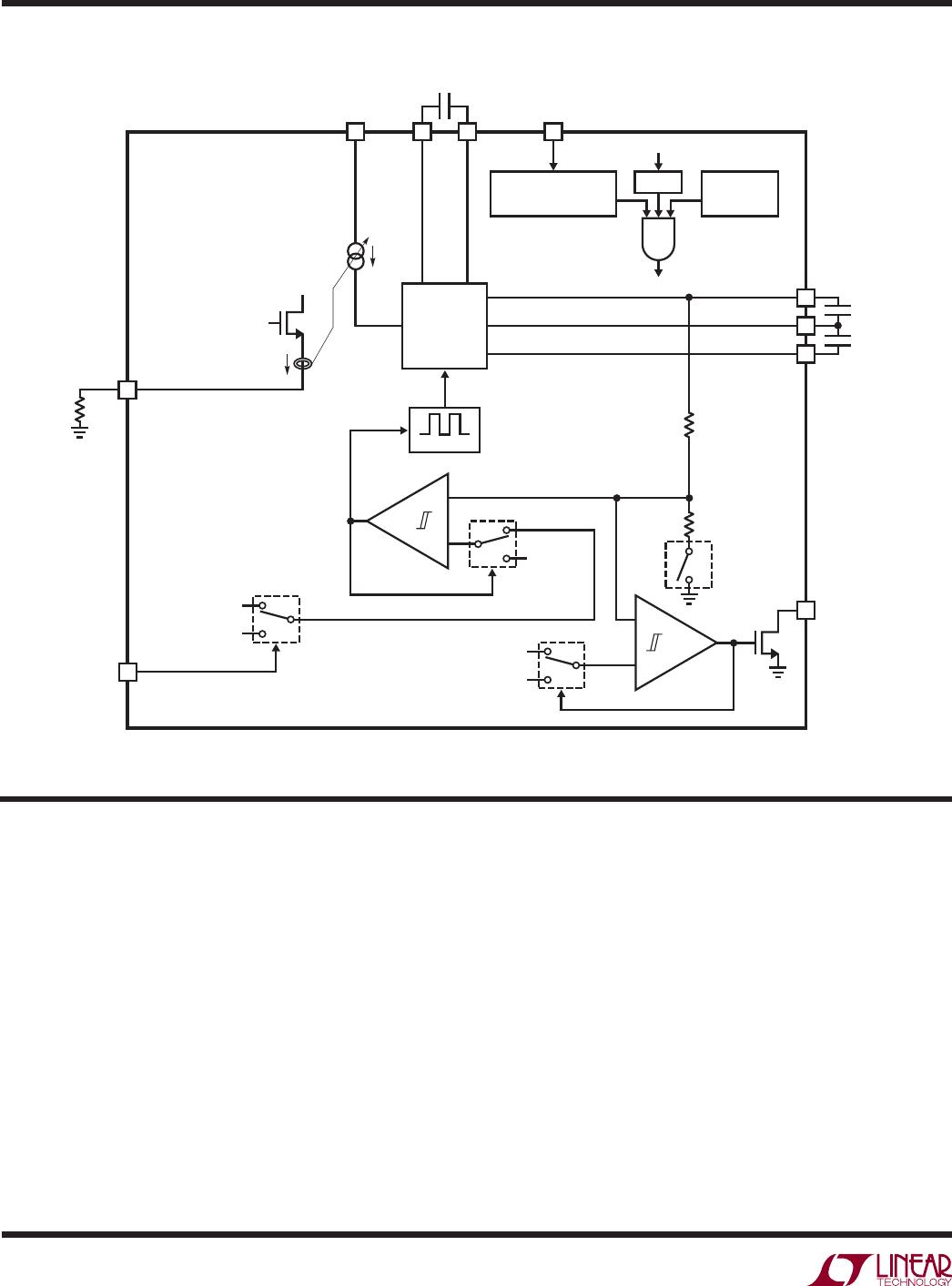
PIN FUNCTIONS
C
+
(Pin 1): Flying Capacitor Positive Terminal. A 1µF X5R
or X7R ceramic capacitor should be connected from C
+
to C
–
.
C
–
(Pin 2): Flying Capacitor Negative Terminal.
CX (Pin 3): Midpoint of Two Series Supercapacitors. This
pin voltage is monitored and forced to track C
OUT
(CX =
C
OUT
/2) during charging to achieve voltage balancing of
the top and bottom supercapacitors.
SHDN (Pin 4): Active Low Shutdown Input. A low on SHDN
puts the LTC3225/LTC3225-1 in low current shutdown
mode. Do not fl oat the SHDN pin.
PGOOD (Pin 5): Open-Drain Output Status Indicator. Upon
start-up, this open-drain pin remains low until the output
voltage, V
OUT
, is within 6% (typical) of its fi nal value. Once
V
OUT
is valid, PGOOD becomes Hi-Z. If V
OUT
falls 7.2%
(typical) below its correct regulation level, PGOOD is
pulled low. PGOOD may be pulled up through an external
resistor to an appropriate reference level. This pin is Hi-Z
in shutdown mode.
V
SEL
(Pin 6): Output Voltage Selection Input. A logic
low at V
SEL
sets the regulated C
OUT
to 4.8V (LTC3225)
or 4V (LTC3225-1); a logic high sets the regulated C
OUT
to 5.3V (LTC3225) or 4.5V (LTC3225-1). Do not fl oat the
V
SEL
pin.
PROG (Pin 7): Charge Current Programming Pin. A resis-
tor connected between this pin and GND sets the charge
current. (See Applications Information section).
GND (Pin 8, Exposed Pad Pin 11): Charge Pump Ground.
These pins must be soldered directly to PCB ground. The
exposed pad must be soldered to a low impedance PCB
ground for rated thermal performance.
V
IN
(Pin 9): Power Supply for the LTC3225/LTC3225-1.
V
IN
should be bypassed to GND with a low ESR ceramic
capacitor of more than 2.2µF.
C
OUT
(Pin 10): Charge Pump Output Pin. Connect C
OUT
to
the top plate of the top supercapacitor. C
OUT
provides charge
current to the supercapacitors and regulates the fi nal volt-
age to 4.8V/5.3V (LTC3225) or 4V/4.5V (LTC3225-1).
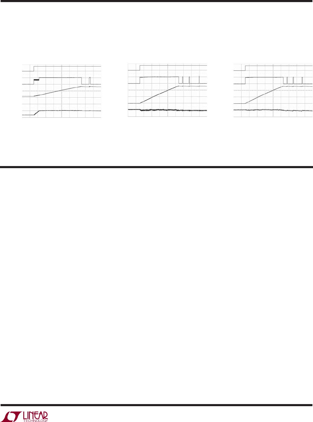
Charging Profi le with Unequal
Initial Output Capacitor Voltage
(Initial V
TOP
= 1V, V
BOT
= 1.3V)
SHDN
5V/DIV
V
COUT
2V/DIV
V
TOP
-V
BOT
500mV/DIV
I
VIN
300mA/DIV
2 SEC/DIV
3225 G10
LTC3225
V
SEL
= V
IN
R
PROG
= 12k
C
TOP
= C
BOT
= 1.1F
C
TOP
INITIAL VOLTAGE = 1V
C
BOT
INITIAL VOLTAGE = 1.3V
SHDN
5V/DIV
V
COUT
2V/DIV
V
TOP
-V
BOT
200mV/DIV
I
VIN
300mA/DIV
5 SEC/DIV
3225 G11
LTC3225
V
SEL
= V
IN
R
PROG
= 12k
C
TOP
= 1.43F
C
BOT
= 1.1F
C
TOP
INITIAL VOLTAGE = 0V
C
BOT
INITIAL VOLTAGE = 0V
SHDN
5V/DIV
V
COUT
2V/DIV
V
TOP
-V
BOT
200mV/DIV
I
VIN
300mA/DIV
5 SEC/DIV
3225 G12
LTC3225
V
SEL
= V
IN
R
PROG
= 12k
C
TOP
= 1.1F
C
BOT
= 1.43F
C
TOP
INITIAL VOLTAGE = 0V
C
BOT
INITIAL VOLTAGE = 0V
Charging Profi le with 30%
Mismatch in Output Capacitance
(C
TOP
> C
BOT
)
Charging Profi le with 30%
Mismatch in Output Capacitance
(C
TOP
< C
BOT
)
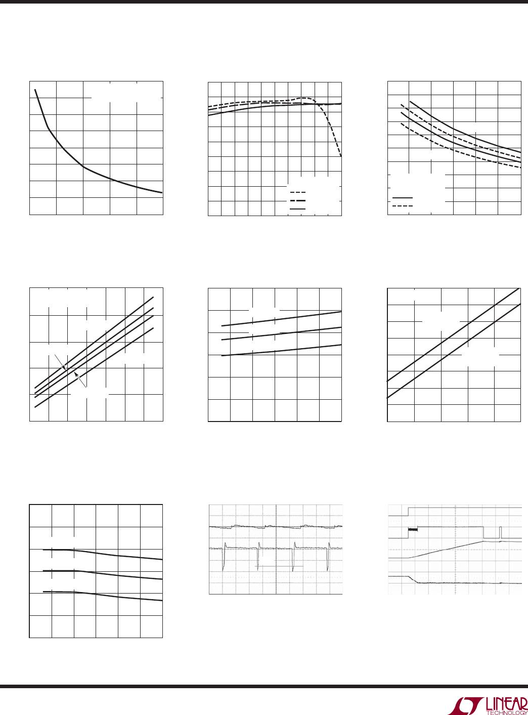
TYPICAL PERFORMANCE CHARACTERISTICS
(T
A
= 25°C, C
FLY
= 1μF, C
IN
= 2.2μF, C
TOP
= C
BOT
, unless otherwise specifi ed)