MAX7426/MAX7427
5th-Order, Lowpass, Elliptic,
Switched-Capacitor
_______________________________________________________________________________________ 7
16.0
16.4
17.2
16.8
17.6
18.0
-40 0 20-20 40 60 80 100
INTERNAL OSCILLATOR FREQUENCY
vs. TEMPERATURE
MAX7426/27-16
TEMPERATURE (°C)
OSCILLATOR FREQUENCY (kHz)
V
DD
= +3V
C
OSC
= 1000pF
V
DD
= +5V
0
6
8
4
2
14
12
10
16
18
20
0 150 20050 100 250 300 350
INTERNAL OSCILLATOR PERIOD
vs. LARGE CAPACITANCE (IN nF)
MAX7426/27-14
CAPACITANCE (nF)
OSCILLATOR PERIOD (ms)
V
DD
= +5V
V
DD
= +3V
17.1
17.2
17.3
17.4
17.5
2.0 3.02.5 3.5 4.0 4.5 5.0 5.5
INTERNAL OSCILLATOR FREQUENCY
vs. SUPPLY VOLTAGE
MAX7426/27-15
SUPPLY VOLTAGE (V)
OSCILLATOR FREQUENCY (kHz)
C
OSC
= 1000pF
-3.5
-2.5
-3.0
-1.5
-2.0
-0.5
-1.0
0
-40 0 20-20 40 60 80 100
DC OFFSET VOLTAGE
vs. TEMPERATURE
MAX7426/27-17
TEMPERATURE (°C)
DC OFFSET VOLTAGE (mV)
V
DD
= +3V
V
DD
= +5V
-4.0
-3.5
-3.0
-2.5
-2.0
-1.5
-1.0
-0.5
0
2.5 3.53.0 4.0 4.5 5.0 5.5
DC OFFSET VOLTAGE
vs. SUPPLY VOLTAGE
MAX7426/27-18
SUPPLY VOLTAGE (V)
DC OFFSET VOLTAGE (mV)
Typical Operating Characteristics (continued)
(V
DD
= +5V for MAX7426, V
DD
= +3V for MAX7427, f
CLK
= 100kHz, SHDN = V
DD
, V
COM
= V
OS
= V
DD
/ 2, T
A
= +25°C, unless other-
wise noted.)
0
50
100
150
200
0 1500 2000500 1000 2500 3000 3500
INTERNAL OSCILLATOR PERIOD
vs. SMALL CAPACITANCE (IN pF)
MAX7426/27-13
CAPACITANCE (pF)
OSCILLATOR PERIOD (µs)
V
DD
= +5V
V
DD
= +3V
MAX7426/MAX7427
5th-Order, Lowpass, Elliptic,
Switched-Capacitor Filters
8 _______________________________________________________________________________________
Detailed Description
The MAX7426/MAX7427 family of 5th-order, elliptic,
lowpass filters provides sharp rolloff with good stop-
band rejection. All parts operate with a 100:1 clock-to-
corner frequency ratio.
Most SCFs are designed with biquadratic sections.
Each section implements two pole-zero pairs, and the
sections can be cascaded to produce higher-order fil-
ters. The advantage to this approach is ease of design.
However, this type of design is highly sensitive to com-
ponent variations if any section’s Q is high. The
MAX7426/MAX7427 use an alternative approach, which
is to emulate a passive network using switched-capaci-
tor integrators with summing and scaling. The passive
network may be synthesized using CAD programs or
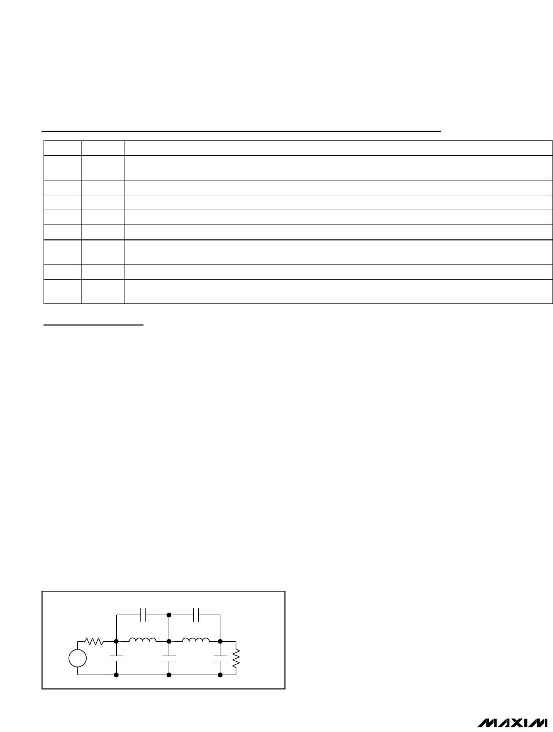
may be found in many filter books. Figure 1 shows a
basic 5th-order ladder elliptic filter structure.
A switched-capacitor filter that emulates a passive lad-
der filter retains many of the same advantages. The
component sensitivity of a passive ladder filter is low
when compared to a cascaded biquadratic design,
because each component affects the entire filter shape
rather than a single pole-zero pair. In other words, a
mismatched component in a biquadratic design has a
concentrated error on its respective poles, while the
same mismatch in a ladder filter design spreads its
error over all poles.
Elliptic Characteristics
Lowpass elliptic filters such as the MAX7426/MAX7427
provide the steepest possible rolloff with frequency of
the four most common filter types (Butterworth, Bessel,
Chebyshev, and elliptic). The high Q value of the poles
near the passband edge combined with the stopband
zeros allow for the sharp attenuation characteristic of
elliptic filters, making these devices ideal for anti-alias-
ing and post-DAC filtering in single-supply systems
(see the Anti-Aliasing and Post-DAC Filtering section).
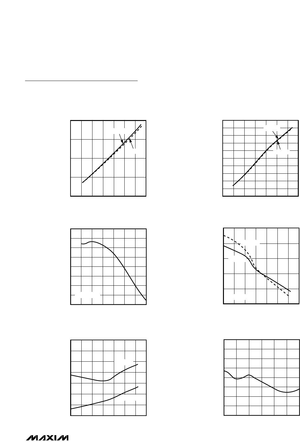
In the frequency domain (Figure 2), the first transmis-
sion zero causes the filter’s amplitude to drop to a mini-
mum level. Beyond this zero, the response rises as the
frequency increases until the next transmission zero.
The stopband begins at the stopband frequency, f
S
. At
frequencies above f
S
, the filter’s gain does not exceed
the gain at f
S
. The corner frequency, f
C
, is defined as
the point where the filter output attenuation falls just
below the passband ripple. The transition ratio (r) is
defined as the ratio of the stopband frequency to the
corner frequency:
r = f
S
/ f
C
The MAX7426/MAX7427 have a transition ratio of 1.25
and typically 37dB of stopband rejection.
Clock Signal
External Clock
These SCFs are designed for use with external clocks
that have a 40% to 60% duty cycle. When using an
external clock, drive the CLK pin with a CMOS gate
C4C2
L4
C5C3C1V
IN
+
-
R
L
L2
R
S
Figure 1. 5th-Order Ladder Elliptic Filter Network
NAME FUNCTION
1 COM
Common Input Pin. Biased internally at midsupply. Bypass externally to GND with a 0.1µF capacitor. To
override internal biasing, drive with an external supply.
2 IN Filter Input
PIN
3 GND Ground
4 V
DD
Positive Supply Input, +5V for MAX7426 or +3V for MAX7427
8 CLK
Clock Input. Connect an external capacitor (C
OSC
) from CLK to GND to set the internal oscillator
frequency. To override the internal oscillator, connect to an external clock.
7
SHDN
Shutdown Input. Drive low to enable shutdown mode; drive high or connect to V
DD
for normal operation.
6 OS
Offset Adjust Input. To adjust output offset, bias OS with a resistive voltage-divider between an external
supply and ground. Connect OS to COM if no offset adjustment is needed.
5 OUT Filter Output
Pin Description
MAX7426/MAX7427
5th-Order, Lowpass, Elliptic,
Switched-Capacitor Filters
_______________________________________________________________________________________ 9
powered from 0 to V
DD
. Varying the rate of the external
clock adjusts the corner frequency of the filter:
Internal Clock
When using the internal oscillator, the capacitance
(C
OSC
) on CLK determines the oscillator frequency:
Since C
OSC
is in the low picofarads, minimize the stray
capacitance at CLK so that it does not affect the inter-
nal oscillator frequency. Varying the rate of the internal
oscillator adjusts the filter’s corner frequency by a
100:1 clock-to-corner frequency ratio. For example, an
internal oscillator frequency of 100kHz produces a
nominal corner frequency of 1kHz.
Input Impedance vs. Clock Frequencies
The MAX7426/MAX7427’s input impedance is effective-
ly that of a switched-capacitor resistor (see the following
equation), and is inversely proportional to frequency.
The input impedance values determined by the equa-
tion represent the average input impedance, since the
input current is not continuous. As a rule, use a driver
with an output resistance less than 10% of the filter’s
input impedance.
Estimate the input impedance of the filter by using the
following formula:
where f
CLK
= clock frequency and C
IN
= 1pF.
Low-Power Shutdown Mode
The MAX7426/MAX7427 have a shutdown mode that is
activated by driving SHDN low. In shutdown mode, the
filter supply current reduces to 0.2µA, and the output of
the filter becomes high impedance. For normal opera-
tion, drive SHDN high or connect to V
DD
.
Applications Information
Offset (OS) and Common-Mode (COM)
Input Adjustment
COM sets the common-mode input voltage and is
biased at midsupply with an internal resistor-divider. If
the application does not require offset adjustment, con-
nect OS to COM. For applications where offset adjust-
ment is required, apply an external bias voltage
through a resistor-divider network to OS, as shown in
Figure 3. For applications that require DC level shifting,
adjust OS with respect to COM. (Note: Do not leave OS
unconnected.) The output voltage is represented by
these equations:
where (V
IN
- V
COM
) is lowpass filtered by the SCF and
OS is added at the output stage. See the Electrical
VVVV
V
V
typical
OUT IN COM OS
COM
DD
( )
()
=− +
=
2
Z
1
f C
IN
CLK IN
=
×
f (kHz)
17.5 10
C (pF)
OSC
3
OSC
=
×
f
f
C
CLK
=
100
PASSBAND STOPBAND
GAIN (dB)
FREQUENCY
f
C
f
S
f
S
f
C
f
S
f
C
TRANSITION RATIO =
RIPPLE
V
DD
V
SUPPLY
IN
CLK
GND
INPUT
OUTPUT
50k
50k
50k
OUT
0.1µF
0.1µF
0.1µF
CLOCK
SHDN
COM
OS
MAX7426
MAX7427
Figure 2. Elliptic Filter Response
Figure 3. Offset Adjustment Circuit

MAX7426CUA+

Mfr. #:
Manufacturer:
Maxim Integrated
Description:
Active Filter 5th-Order Lowpass Elliptic Filter
Lifecycle:
New from this manufacturer.
Delivery:
DHL FedEx Ups TNT EMS
Payment:
T/T Paypal Visa MoneyGram Western Union