Operation M41T0
10/23 Doc ID 9105 Rev 7
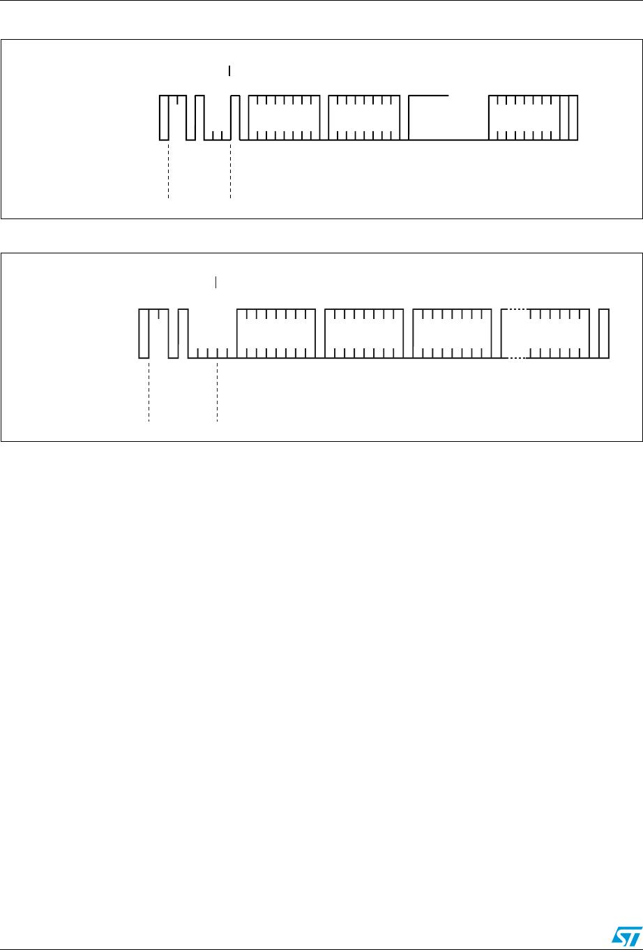
2.2 READ mode
In this mode, the master reads the M41T0 slave after setting the slave address (see
Figure 7). Following the WRITE mode control bit (R/W
= 0) and the acknowledge bit, the
word address An is written to the on-chip address pointer. Next the START condition and
slave address are repeated, followed by the READ mode control bit (R/W
= 1). At this point,
the master transmitter becomes the master receiver. The data byte which was addressed
will be transmitted and the master receiver will send an acknowledge bit to the slave
transmitter. The address pointer is only incremented on reception of an acknowledge bit.
The M41T0 slave transmitter will now place the data byte at address A
n+1
on the bus. The
master receiver reads and acknowledges the new byte and the address pointer is
incremented to A
n+2
.
This cycle of reading consecutive addresses will continue until the master receiver sends a
STOP condition to the slave transmitter.
An alternate READ mode may also be implemented, whereby the master reads the M41T0
slave without first writing to the (volatile) address pointer. The first address that is read is the
last one stored in the pointer (see Figure 9 on page 12).
Table 2. AC characteristics
Symbol Parameter
(1)
1. Valid for ambient operating temperature: T
A
= –40 to 85 °C; V
CC
= 2.0 to 5.5 V (except where noted).
Min Typ Max Unit
f
SCL
SCL clock frequency 0 400 kHz
t
LOW
Clock low period 1.3 µs
t
HIGH
Clock high period 600 ns
t
R
SDA and SCL rise time 300 ns
t
F
SDA and SCL fall time 300 ns
t
HD:STA
START condition hold time
(after this period the first clock pulse is generated)
600 ns
t
SU:STA
START condition setup time
(only relevant for a repeated start condition)
600 ns
t
SU:DAT
Data setup time 100 ns
t
HD:DAT
(2)
2. Transmitter must internally provide a hold time to bridge the undefined region (300 ns max.) of the falling
edge of SCL.
Data hold time 0 µs
t
SU:STO
STOP condition setup time 600 ns
t
BUF
Time the bus must be free before a new transmission
can start
1.3 µs