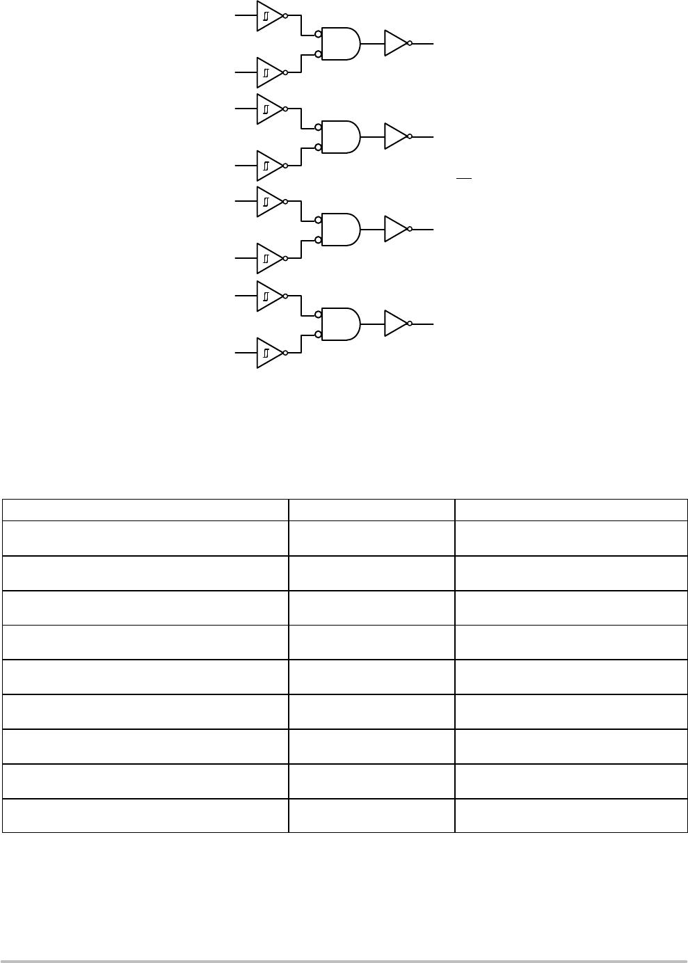
NLV74HC132ADR2G

© Semiconductor Components Industries, LLC, 2013
May, 2013 Rev. 15
1 Publication Order Number:
MC74HC132A/D
MC74HC132A
Quad 2-Input NAND Gate
with Schmitt-Trigger Inputs
HighPerformance SiliconGate CMOS
The MC74HC132A is identical in pinout to the LS132. The device
inputs are compatible with standard CMOS outputs; with pullup
resistors, they are compatible with LSTTL outputs.
The HC132A can be used to enhance noise immunity or to square up
slowly changing waveforms.
Features
Output Drive Capability: 10 LSTTL Loads
Outputs Directly Interface to CMOS, NMOS, and TTL
Operating Voltage Range: 2.0 to 6.0 V
Low Input Current: 1.0 mA
High Noise Immunity Characteristic of CMOS Devices
In Compliance with the Requirements as Defined by JEDEC
Standard No. 7A
Chip Complexity: 72 FETs or 18 Equivalent Gates
NLV Prefix for Automotive and Other Applications Requiring
Unique Site and Control Change Requirements; AECQ100
Qualified and PPAP Capable
These Devices are PbFree, Halogen Free/BFR Free and are RoHS
Compliant
Figure 1. Pin Assignment
11
12
13
14
8
9
105
4
3
2
1
7
6
B3
Y4
A4
B4
V
CC
Y3
A3
A2
Y1
B1
A1
GND
Y2
B2
See detailed ordering and shipping information in the package
dimensions section on page 2 of this data sheet.
ORDERING INFORMATION
Inputs Output
ABY
LLH
LHH
HLH
HHL
FUNCTION TABLE
http://onsemi.com
MARKING
DIAGRAMS
A = Assembly Location
L, WL = Wafer Lot
Y, YY = Year
W, WW = Work Week
G or G = PbFree Package
TSSOP14
DT SUFFIX
CASE 948G
14
1
SOIC14
D SUFFIX
CASE 751A
14
1
HC132AG
AWLYWW
1
14
HC
132A
ALYWG
G
1
14
14
1
PDIP14
N SUFFIX
CASE 646
MC74HC132AN
AWLYYWWG
1
14
(Note: Microdot may be in either location)
MC74HC132A
http://onsemi.com
2
Figure 2. Logic Diagram
A1
B1
Y1
3
2
1
PIN 14 = V
CC
PIN 7 = GND
Y = AB
A2
B2
Y2
6
5
4
A3
B3
Y3
8
10
9
A4
B4
Y4
11
13
12
ORDERING INFORMATION
Device Package Shipping
MC74HC132ANG PDIP14
(PbFree)
25 / Tape & Ammo Box
MC74HC132ADG SOIC14
(PbFree)
55 Units / Rail
MC74HC132ADR2G SOIC14
(PbFree)
2500 / Tape & Reel
MC74HC132ADTG TSSOP14
(PbFree)
96 Units / Rail
MC74HC132ADTR2G TSSOP14
(PbFree)
2500 / Tape & Reel
NLV74HC132ADG* SOIC14
(PbFree)
55 Units / Rail
NLV74HC132ADR2G* SOIC14
(PbFree)
2500 / Tape & Reel
NLV74HC132ADTG* TSSOP14
(PbFree)
96 Units / Rail
NLV74HC132ADTR2G* TSSOP14
(PbFree)
2500 / Tape & Reel
For information on tape and reel specifications, including part orientation and tape sizes, please refer to our Tape and Reel Packaging
Specifications Brochure, BRD8011/D.
*NLV Prefix for Automotive and Other Applications Requiring Unique Site and Control Change Requirements; AECQ100 Qualified and PPAP
Capable
MC74HC132A
http://onsemi.com
3
MAXIMUM RATINGS
Symbol Parameter Value Unit
V
CC
Positive DC Supply Voltage 0.5 to 7.0 V
V
IN
Digital Input Voltage 0.5 to 7.0 V
V
OUT
DC Output Voltage Output in 3State
High or Low State
0.5 to 7.0
0.5 to V
CC
0.5
V
I
IK
Input Diode Current 20 mA
I
OK
Output Diode Current 20 mA
I
OUT
DC Output Current, per Pin 25 mA
I
CC
DC Supply Current, V
CC
and GND Pins 75 mA
I
GND
DC Ground Current per Ground Pin 75 mA
T
STG
Storage Temperature Range 65 to 150
_C
T
L
Lead Temperature, 1 mm from Case for 10 Seconds 260
_C
T
J
Junction Temperature Under Bias 150
_C
q
JA
Thermal Resistance 14PDIP
14SOIC
14TSSOP
78
125
170
_C/W
P
D
Power Dissipation in Still Air at 85_C PDIP
SOIC
TSSOP
750
500
450
mW
MSL Moisture Sensitivity Level 1
F
R
Flammability Rating Oxygen Index: 30% 35% UL 94 V0 @ 0.125 in
V
ESD
ESD Withstand Voltage Human Body Model (Note 1)
Machine Model (Note 2)
Charged Device Model (Note 3)
2000
100
500
V
I
LatchUp
LatchUp Performance Above V
CC
and Below GND at 85_C (Note 4)
300 mA
Stresses exceeding Maximum Ratings may damage the device. Maximum Ratings are stress ratings only. Functional operation above the
Recommended Operating Conditions is not implied. Extended exposure to stresses above the Recommended Operating Conditions may affect
device reliability.
1. Tested to EIA/JESD22A114A.
2. Tested to EIA/JESD22A115A.
3. Tested to JESD22C101A.
4. Tested to EIA/JESD78.
RECOMMENDED OPERATING CONDITIONS
Symbol Parameter Min Max Unit
V
CC
DC Supply Voltage (Referenced to GND) 2.0 6.0 V
V
IN
, V
OUT
DC Input Voltage, Output Voltage (Referenced to GND) 0 V
CC
V
T
A
Operating Temperature, All Package Types 55 125
_C
t
r
, t
f
Input Rise and Fall Time (Figure 3) No Limit
(Note 5)
ns
5. When V
IN
0.5 V
CC
, I
CC
>> quiescent current.
6. Unused inputs may not be left open. All inputs must be tied to a highlogic voltage level or a lowlogic input voltage level.

NLV74HC132ADR2G

Mfr. #:
Manufacturer:
ON Semiconductor
Description:
Logic Gates QUAD 2-INPUT NAND SC
Lifecycle:
New from this manufacturer.
Delivery:
DHL FedEx Ups TNT EMS
Payment:
T/T Paypal Visa MoneyGram Western Union