ZVN3306FTA

SOT23 N-CHANNEL ENHANCEMENT
MODE VERTICAL DMOS FET
ISSUE 3 – JANUARY 1996
FEATURES
*R
DS(on)
=5
* 60 Volt V
DS
COMPLEMENTARY TYPE - ZVP3306F
PARTMARKING DETAIL - MC
ABSOLUTE MAXIMUM RATINGS.
PARAMETER SYMBOL VALUE UNIT
Drain-Source Voltage V
DS
60 V
Continuous Drain Current at T
amb
=25°C I
D
150 mA
Pulsed Drain Current I
DM
3A
Gate-Source Voltage V
GS
± 20
V
Power Dissipation at T
amb
=25°C P
tot
330 mW
Operating and Storage Temperature Range T
j
:T
stg
-55 to +150 °C
ELECTRICAL CHARACTERISTICS (at T
amb
= 25°C unless otherwise stated).
PARAMETER SYMBOL MIN. MAX. UNIT CONDITIONS.
Drain-Source
Breakdown Voltage
BV
DSS
60 V I
D
=1mA, V
GS
=0V
Gate-Source Threshold
Voltage
V
GS(th)
0.8 2.4 V I
D
=1mA, V
DS
=V
GS
Gate-Body Leakage I
GSS
20 nA
V
GS
=± 20V, V
DS
=0V
Zero Gate Voltage
Drain Current
I
DSS
0.5
50
µA
µA
V
DS
=60V, V
GS
=0V
V
DS
=48V, V
GS
=0V, T=125°C(2)
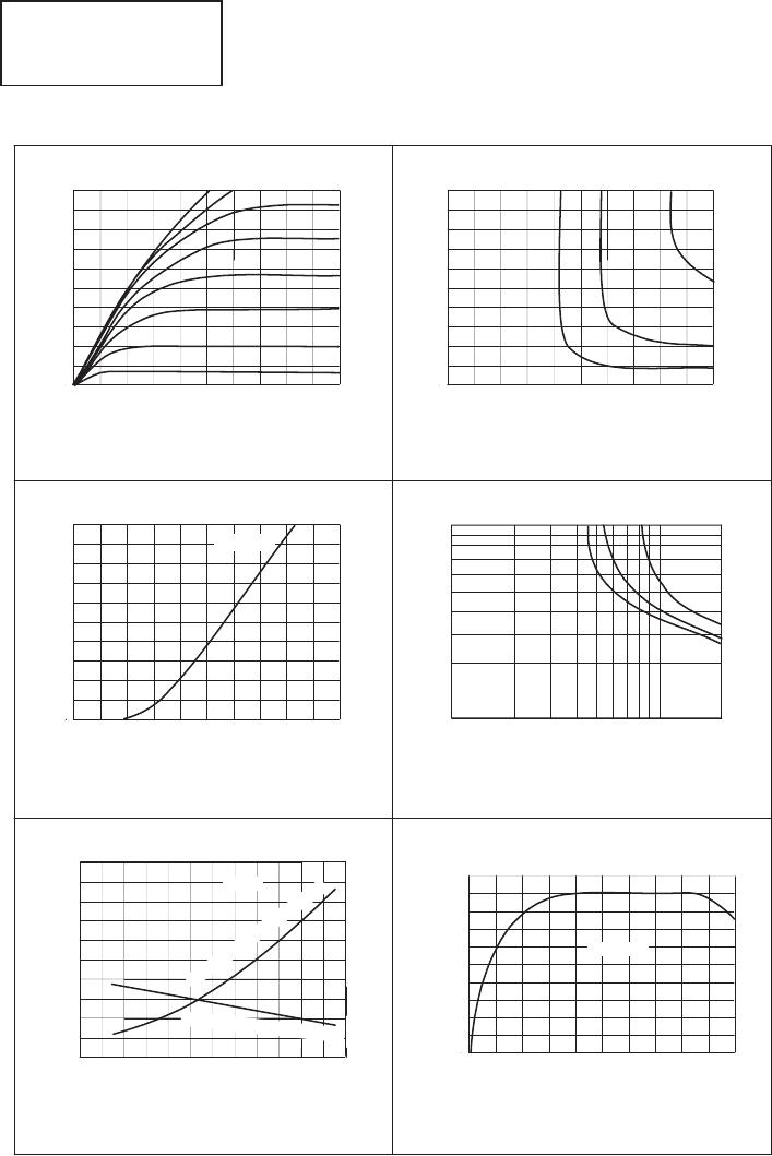
On-State Drain Current(1) I
D(on)
750 mA V
DS
=18V, V
GS
=10V
Static Drain-Source On-State
Resistance (1)
R
DS(on)
5
V
GS
=10V, I
D
=500mA
Forward Transconductance
(1)(2)
g
fs
150 mS V
DS
=18V, I
D
=500mA
Input Capacitance (2) C
iss
35 pF
Common Source
Output Capacitance (2)
C
oss
25 pF V
DS
=18V, V
GS
=0V, f=1MHz
Reverse Transfer Capacitance
(2)
C
rss
8pF
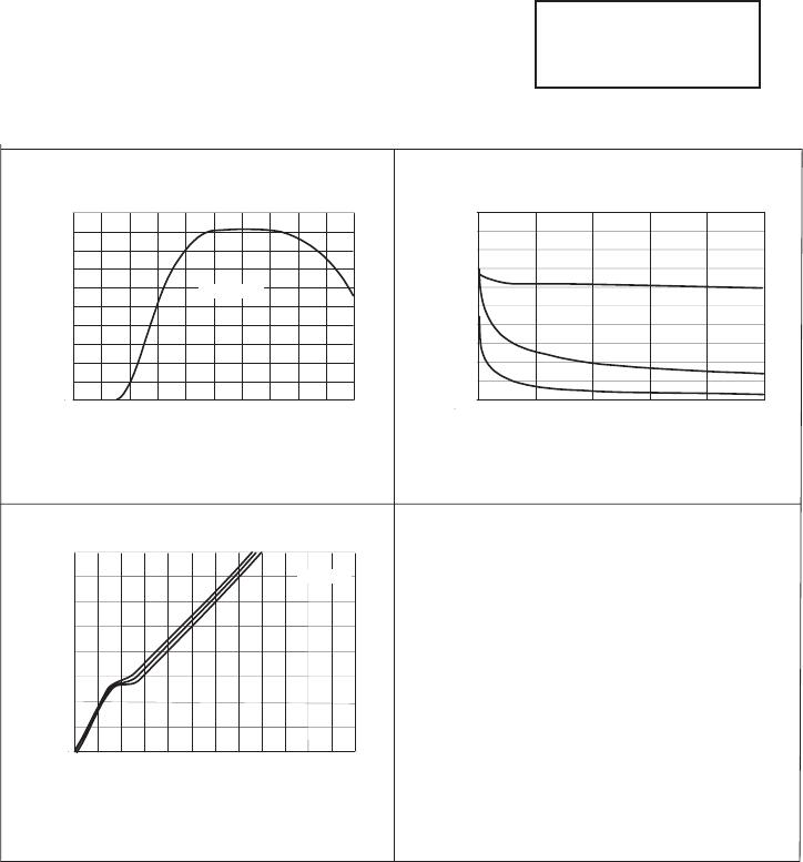
Turn-On Delay Time (2)(3) t
d(on)
3typ 5 ns
V
DD
18V, I
D
=500mA
Rise Time (2)(3) t
r
4typ 7 ns
Turn-Off Delay Time (2)(3) t
d(off)
4typ 6 ns
Fall Time (2)(3) t
f
5typ 8 ns
(1) Measured under pulsed conditions. Width=300µs. Duty cycle 2% (2) Sample test.
(3) Switching times measured with 50source impedance and <5ns rise time on a pulse generator
Spice parameter data is available upon request for this device
ZVN3306F
D
G
S
SOT23
3 - 393
TYPICAL CHARACTERISTICS
VDS - Drain Source Voltage (Volts)
I
D(O
n
)
-On-State Drain Current
(Amps)
Transfer Characteristics
Saturation Characteristics
V
DS-
Drain Source
Voltage (Volts)
Voltage Saturation Characteristics
VGS-
Gate Source Voltage
(Volts)
ID=
1A
0.5A
0.25A
I
D(
O
n
)
-
On-
Stat
e
Drain Cur
r
e
n
t (
Am
ps)
VGS -Gate Source Voltage (Volts)
0.6
0
0.2
0.4
0.8
02 4 6 8 10
1.0
VGS=10V
5V
7V
8V
6V
4V
3V
9V
Normalised R
DS(on)
and V
GS(th)
vs Temperature
Nor
m
ali
s
e
d
R
DS(on)
a
nd V
G
S(th)
-40
-20 0 20 40 60 80
120
100 140 160
2.4
2.2
2.0
1.8
1.6
1.4
1.2
1.0
0.6
0.8
Dr
ain-S
o
u
rc
e R
e
s
i
s
tance
R
D
S(o
n
)
G
ate
T
h
res
h
o
l
d
V
o
l
t
ag
e
V
GS(
th
)
ID=-0.5A
T-Temperature (C°)
0.4
-80
-60
0.6
0
0.2
0.4
0.8
02 4 6 8 10
1.0
6
0
2
4
8
02 4 6 8 10
10
On-resistance vs gate-source voltage
VGS-Gate Source Voltage (Volts)
R
DS(ON)
-Drain Source Resistance
()
11020
1
10
5
Transconductance v drain current
ID(on) - Drain Current (Amps
)
g
fs
-Fo
r
war
d
T
r
a
nsc
o
ndu
ctance (mS)
0 0.1 0.2 0.3 0.4 0.5 0.6 0.7 0.8 0.9 1.0
0
VDS=18V
60
40
20
80
160
140
120
100
180
200
VDS=10V
ID=
1A
0.5A
0.25A
ZVN3306F
3 - 394
TYPICAL CHARACTERISTICS
0
Q-Charge (nC)
Transconductance v gate-source voltage
V
GS
-Gate Source Voltage (Volts)
V
G
S
-Gate Source Voltage (V
olts)
Gate charge v gate-source voltage
10
8
6
2
0
4
12
14
16
V
DD
=20V
I
D=
800mA
30V
50V
0.2 0.4 0.6 0.8 1.0 1.2 1.4 1.6 1.8 2.0 2.2 2.4
g
fs
-
T
r
an
sc
o
nd
ucta
nce (mS)
V
DS
-Drain Source Voltage (Volts)
Capacitance v drain-source voltage
C-Capacitance (pF)
C
oss
C
iss
C
rss
0
10 20
30
40 50
0
30
20
10
40
50
012345678910
0
V
DS=
18V
60
40
20
80
160
140
120
100
180
200
ZVN3306F
3 - 395

ZVN3306FTA

Mfr. #:
Manufacturer:
Diodes Incorporated
Description:
MOSFET N-Chnl 60V
Lifecycle:
New from this manufacturer.
Delivery:
DHL FedEx Ups TNT EMS
Payment:
T/T Paypal Visa MoneyGram Western Union

Products related to this Datasheet