Application Specific Quick Turn Clock
TM
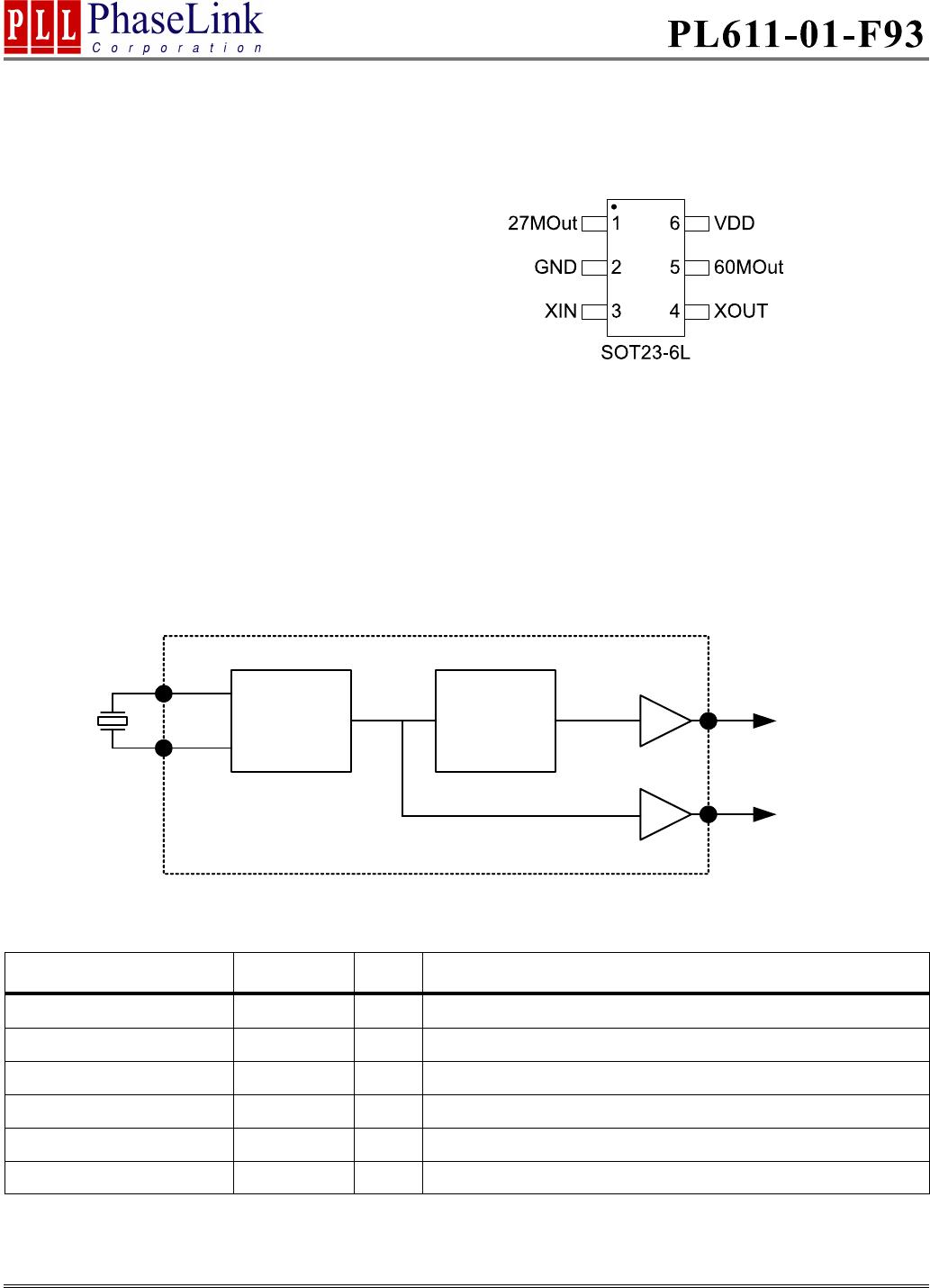
For use with Sigma Designs SMP8644/42 and SMP8654/52
47745 Fremont Blvd., Fremont, California 94538 Tel (510) 492-0990 Fax (510) 492-0991 www.phaselink.com Rev 5/13/09 Page 3
PACKAGE DRAWING (GREEN PACKAGE COMPLIANT)
ORDERING INFORMATION (GREEN PACKAGE COMPLIANT)
PhaseLink Corporation, reserves the right to make changes in its products or specifications, or both at any time without notice. The information
furnished by Phaselink is believed to be accurate and reliable. However, PhaseLink makes no guarantee or warranty concerning the accuracy of said
information and shall not be responsible for any loss or damage of whatever nature resulting from the use of, or reliance upon this product.
LIFE SUPPORT POLICY: PhaseLink’s products are not authorized for use as critical components in life support devices or systems without the
express written approval of the President of PhaseLink Corporation.
For part ordering, please contact our Sales Department:
47745 Fremont Blvd., Fremont, CA 94538, USA
Tel: (510) 492-0990 Fax: (510) 492-0991
PART NUMBER
The order number for this device is a combination of the following:
Part number, Package type and Operating temperature range
Part Number
Package Type
T=SOT23-6L
Temperature Range
C=Commercial (0°C to 70°C)
Shipping Option
Blank=Tube
R=Tape & Reel
Part / Order Number Marking* Package Option
PL611-01-F93TC-R
C1F93
LLL
6-Pin SOT-23 (Tape and Reel)
*Note: LLL represents the production lot number
Recommended Land Pattern (MM)
2.35
1.905
0.915
±0.05
1.473
0.95
0.482
±0.050
3.785
±0.05
E
H
D
Pin1 Dot
C
L
A2
A1
e
b
A
Min Max
A 1.05 1.45
A1 0.05 0.15
A2 1.00 1.30
b 0.35 0.50
c
D 2.80 3.00
E 1.50 1.70
H 2.60 3.00
L 0.35 0.55
e
Symbol
Dimension (MM)
0.127 Typical
0.95 Typical
SOT23-6L