48
Integrated Silicon Solution, Inc. — www.issi.com —
1-800-379-4774
PRELIMINARY INFORMATION Rev. 00J
03/03/09
IS42S32400B
DON'T CARE
CLK
COMMAND
BANK n
BANK m
ADDRESS
DQ
T0 T1 T2 T3 T4 T5 T6 T7
NOP NOP NOP NOP NOP NOP
DOUT a
DOUT a+1
DOUT b
DOUT b+1
BANK n,
COL a
CAS Latency - 3 (BANK n)
CAS Latency - 3 (BANK m)
tRP - BANK n tRP - BANK m
READ - AP
BANK n
READ - AP
BANK m
Page Active READ with Burst of 4 Interrupt Burst, Precharge Idle
Page Active READ with Burst of 4 Precharge
Internal States
BANK n,
COL b
DON'T CARE
CLK
COMMAND
BANK n
BANK m
ADDRESS
DQM
DQ
T0 T1 T2 T3 T4 T5 T6 T7
NOP NOP NOP NOP NOP NOP
D
OUT
a
D
IN
b
D
IN
b+1
D
IN
b+2
D
IN
b+3
BANK n,
COL a
BANK m,
COL b
CAS Latency - 3 (BANK n)
t
RP - BANK n
t
DP L - BANK m
READ - AP
BANK n
WRITE - AP
BANK m
READ with Burst of 4 Interrupt Burst, Precharge Idle
Page Active WRITE with Burst of 4 Write-Back
Internal States
Page Active
BURST READ/SINGLE WRITE
The burst read/single write mode is entered by programming
the write burst mode bit
(M9)
in the mode register to a logic 1.
In this mode, all
WRITE
commands result in the access of a
single column location (burst of one), regardless of the
programmed burst length. READ commands access
columns according to the programmed burst length and
sequence, just as in the normal mode of operation (M9 = 0).
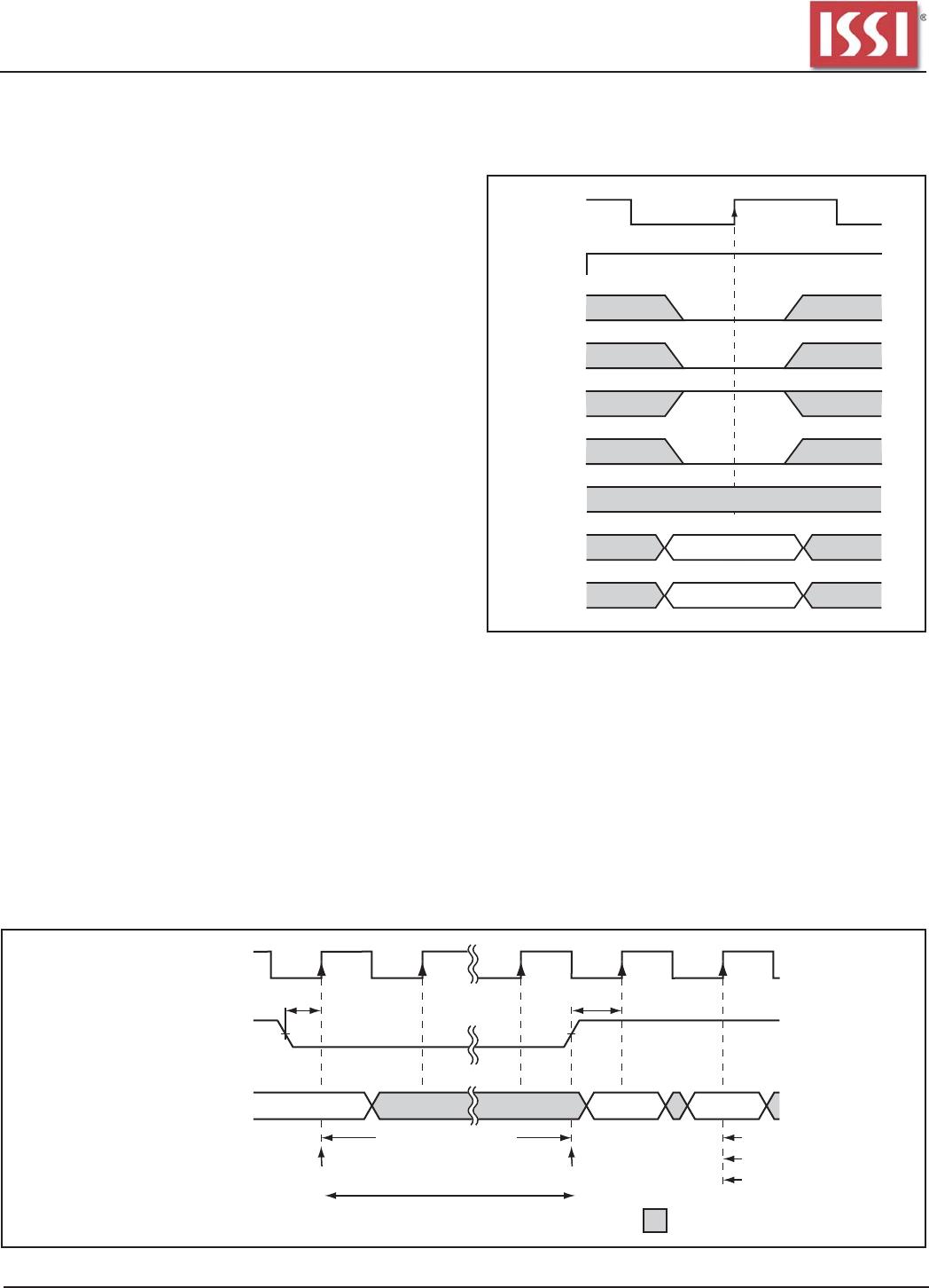
CONCURRENT AUTO PRECHARGE
An access command (READ or WRITE) to another bank
while an access command with auto precharge enabled is
executing is not allowed by SDRAMs, unless the SDRAM
supports CONCURRENT AUTO PRECHARGE. ISSI
SDRAMs support CONCURRENT AUTO PRECHARGE.
Four cases where CONCURRENT AUTO PRECHARGE
occurs are defined below.
READ with Auto Precharge
1. Interrupted by a READ (with or without auto precharge):
A READ to bank m will interrupt a READ on bank n, CAS
latency later. The PRECHARGE to bank n will begin
when the READ to bank m is registered.
2. Interrupted by a WRITE (with or without auto precharge):
A WRITE to bank m will interrupt a READ on bank n when
registered. DQM should be used three clocks prior to the
WRITE command to prevent bus contention. The
PRECHARGE to bank n will begin when the WRITE to
bank m is registered.
READ With Auto Precharge interrupted by a READ
READ With Auto Precharge interrupted by a WRITE