LT1208/LT1209
6
CCHARA TERIST
ICS
UW
AT
Y
P
I
CA
LPER
F
O
R
C
E
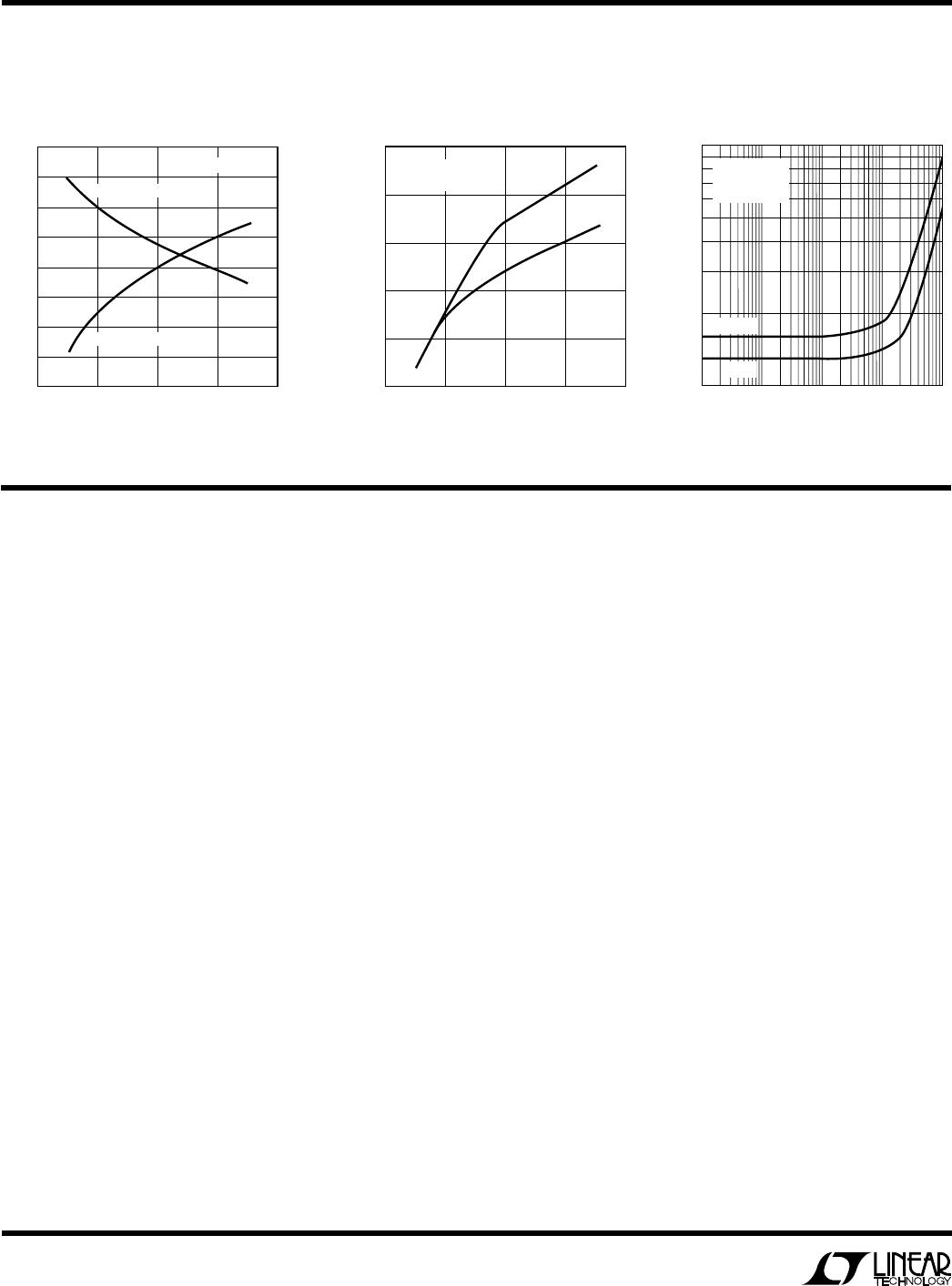
Gain-Bandwidth and Phase Margin Total Harmonic Distortion
vs Supply Voltage Slew Rate vs Supply Voltage vs Frequency
U
S
A
O
PP
L
IC
AT
I
WU
U
I FOR ATIO
Layout and Passive Components
As with any high speed operational amplifier, care must be
taken in board layout in order to obtain maximum perfor-
mance. Key layout issues include: use of a ground plane,
minimization of stray capacitance at the input pins, short
lead lengths, RF-quality bypass capacitors located close
to the device (typically 0.01µF to 0.1µF), and use of low
ESR bypass capacitors for high drive current applications
(typically 1µF to 10µF tantalum). Sockets should be
avoided when maximum frequency performance is re-
quired, although low profile sockets can provide reason-
able performance up to 50MHz. For more details see
Design Note 50. The parallel combination of the feedback
resistor and gain setting resistor on the inverting input
combine with the input capacitance to form a pole which
can cause peaking. If feedback resistors greater than 5k
are used, a parallel capacitor of value
C
F
≥ R
G
× C
IN
/R
F
should be used to cancel the input pole and optimize
dynamic performance. For unity-gain applications where
a large feedback resistor is used, C
F
should be greater than
or equal to C
IN
.
Capacitive Loading
The LT1208/LT1209 amplifiers are stable with capacitive
loads. This is accomplished by sensing the load induced
output pole and adding compensation at the amplifier gain
node. As the capacitive load increases, both the bandwidth
and phase margin decrease so there will be peaking in the
frequency domain and in the transient response. The
photo of the small-signal response with 1000pF load
shows 50% peaking. The large-signal response with a
10,000pF load shows the output slew rate being limited by
the short-circuit current. To reduce peaking with capaci-
tive loads, insert a small decoupling resistor between the
output and the load, and add a capacitor between the
output and inverting input to provide an AC feedback path.
Coaxial cable can be driven directly, but for best pulse
fidelity the cable should be doubly terminated with a
resistor in series with the output.
SUPPLY VOLTAGE (±V)
0
GAIN-BANDWIDTH (MHz)
20
1208/09 G19
5
10
15
60
55
50
45
40
35
30
25
20
62
60
58
56
54
52
50
48
46
PHASE MARGIN (DEG)
PHASE MARGIN
GAIN BANDWIDTH
T
A
= 25°C
SUPPLY VOLTAGE (±V)
0
SLEW RATE (V/µs)
20
1208/09 G20
5
10
15
600
500
400
300
200
100
–SR
+SR
T
A
= 25°C
A
V
= –1
FREQUENCY (Hz)
0.001
TOTAL HARMONIC DISTORTION (%)
0.01
10 1k 10k
1208/09 G21
100 100k
A
V
= –1
A
V
= 1
T
A
= 25°C
V
OUT
= 3V
RMS
R
L
= 500Ω