MM5Z2V4T1 SERIES
http://onsemi.com
3
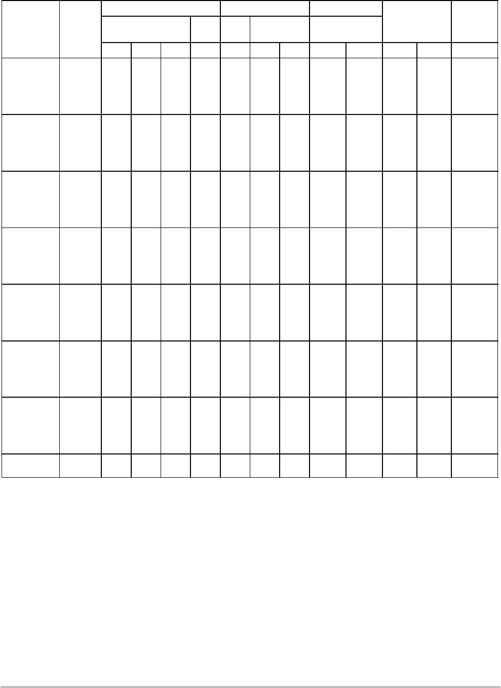
ELECTRICAL CHARACTERISTICS (T
A
= 25°C unless otherwise noted, V
F
= 0.9 V Max. @ I
F
= 10 mA for all types)
Zener Voltage (Note 1) Zener Impedance Leakage Current
V
Z
(Volts) @ I
ZT
Z
ZT
@ I
ZT
Z
ZK
@ I
ZK
I
R
@ V
R
Z
(mV/k)
@ I
ZT
@ V
R
= 0
f = 1 MHz
Device
ev
ce
Marking
Min Nom Max mA mA A Volts Min Max pF
MM5Z2V4T1 00 2.2 2.4 2.6 5 100 1000 1.0 50 1.0 −3.5 0 450
MM5Z2V7T1 01 2.5 2.7 2.9 5 100 1000 1.0 20 1.0 −3.5 0 450
MM5Z3V0T1 02 2.8 3.0 3.2 5 100 1000 1.0 10 1.0 −3.5 0 450
MM5Z3V3T1 05 3.1 3.3 3.5 5 95 1000 1.0 5 1.0 −3.5 0 450
MM5Z3V6T1 06 3.4 3.6 3.8 5 90 1000 1.0 5 1.0 −3.5 0 450
MM5Z3V9T1 07 3.7 3.9 4.1 5 90 1000 1.0 3 1.0 −3.5 −2.5 450
MM5Z4V3T1 08 4.0 4.3 4.6 5 90 1000 1.0 3 1.0 −3.5 0 450
MM5Z4V7T1 09 4.4 4.7 5.0 5 80 800 1.0 3 2.0 −3.5 0.2 260
MM5Z5V1T1 0A 4.8 5.1 5.4 5 60 500 1.0 2 2.0 −2.7 1.2 225
MM5Z5V6T1 0C 5.2 5.6 6.0 5 40 200 1.0 1 2.0 −2.0 2.5 200
MM5Z6V2T1 0E 5.8 6.2 6.6 5 10 100 1.0 3 4.0 0.4 3.7 185
MM5Z6V8T1 0F 6.4 6.8 7.2 5 15 160 1.0 2 4.0 1.2 4.5 155
MM5Z7V5T1 0G 7.0 7.5 7.9 5 15 160 1.0 1 5.0 2.5 5.3 140
MM5Z8V2T1 0H 7.7 8.2 8.7 5 15 160 1.0 0.7 5.0 3.2 6.2 135
MM5Z9V1T1 0K 8.5 9.1 9.6 5 15 160 1.0 0.2 7.0 3.8 7.0 130
MM5Z10VT1 0L 9.4 10 10.6 5 20 160 1.0 0.1 8.0 4.5 8.0 130
MM5Z11VT1 0M 10.4 11 11.6 5 20 160 1.0 0.1 8.0 5.4 9.0 130
MM5Z12VT1 0N 11.4 12 12.7 5 25 80 1.0 0.1 8.0 6.0 10 130
MM5Z13VT1 0P 12.4 13.25 14.1 5 30 80 1.0 0.1 8.0 7.0 11 120
MM5Z15VT1 0T 14.3 15 15.8 5 30 80 1.0 0.05 10.5 9.2 13 110
MM5Z16VT1 0U 15.3 16.2 17.1 2 40 80 1.0 0.05 11.2 10.4 14 105
MM5Z18VT1 0W 16.8 18 19.1 2 45 80 1.0 0.05 12.6 12.4 16 100
MM5Z20VT1 0Z 18.8 20 21.2 2 55 100 1.0 0.05 14.0 14.4 18 85
MM5Z22VT1 10 20.8 22 23.3 2 55 100 1.0 0.05 15.4 16.4 20 85
MM5Z24VT1 11 22.8 24.2 25.6 2 70 120 1.0 0.05 16.8 18.4 22 80
MM5Z27VT1 12 25.1 27 28.9 2 80 300 1.0 0.05 18.9 21.4 25.3 70
MM5Z30VT1 14 28 30 32 2 80 300 1.0 0.05 21.0 24.4 29.4 70
MM5Z33VT1 18 31 33 35 2 80 300 1.0 0.05 23.2 27.4 33.4 70
MM5Z36VT1 19 34 36 38 2 90 500 1.0 0.05 25.2 30.4 37.4 70
MM5Z39VT1 20 37 39 41 2 130 500 1.0 0.05 27.3 33.4 41.2 45
MM5Z43VT1 21 40 43 46 1 150 500 1.0 0.05 30.1 37.6 46.6 40
MM5Z47VT1 1A 44 47 50 1 170 500 1.0 0.05 32.9 42.0 51.8 40
MM5Z51VT1 1C 48 51 54 1 180 500 1.0 0.05 35.7 46.6 57.2 40
MM5Z56VT1 1D 52 56 60 1 200 500 1.0 0.05 39.2 52.2 63.8 40
MM5Z62VT1 1E 58 62 66 1 215 500 1.0 0.05 43.4 58.8 71.6 35
MM5Z68VT1 1F 64 68 72 1 240 500 1.0 0.05 47.6 65.6 79.8 35
MM5Z75VT1 1G 70 75 79 1 255 500 1.0 0.05 52.5 73.4 88.6 35
1. Zener voltage is measured with a pulse test current I
Z
at an ambient temperature of 25°C.