Expand menu
Hello, Sign in
My Account
0
Cart
Home
Products
Sensors
Semiconductors
Passive Components
Connectors
Power
Electromechanical
Optoelectronics
Circuit Protection
Integrated Circuits - ICs
Main Products
Manufacturers
Blog
Services
About OMO
About Us
Contact Us
Check Stock
TL594CDTBG
P1-P3
P4-P6
P7-P9
P10-P12
TL594
http://onsemi.com
7
Figure 1
1. Error−Amplifier Characteristics
Figure 12. Deadtime and Feedback Control Circuit
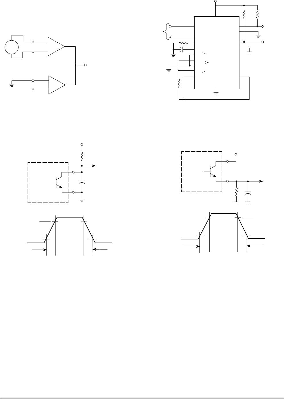
Figure 13. Common−Emitter Configuration
T
est Circuit and W
aveform
+
+
V
in
Error Amplifier
Under T
est
Feedback
T
erminal
(Pin 3)
Other Error
Amplifier
V
ref
V
CC
= 15V
150
2W
Output 1
Output 2
C1
E1
C2
E2
Ref
Out
Gnd
Output
Control
(+)
(+)
(−)
(−)
Feedback
Deadtime
Error
V
CC
T
est
Inputs
50k
R
T
C
T
150
2W
Figure 14. Emitter−Follower Configuration
T
est Circuit and W
aveform
R
L
68
V
C
C
L
15pF
C
E
Q
Each
Output
Transistor
15V
90%
V
CC
10%
90%
10%
t
r
t
f
R
L
68
V
EE
C
L
15pF
C
E
Q
Each
Output
Transistor
15V
90%
V
EE
10%
90%
10%
t
r
t
f
−
−
Gnd
TL594
http://onsemi.com
8
Figure 15. Error−Amplifier Sensing T
echniques
Figure 16. Deadtime
Control Circuit
Figure 17. Soft−Start Circuit
Figure 18. Output Connections for Single−Ended and Push−Pull Configurations
V
O
T
o Output
V
oltage of
System
R1
1
2
V
ref
R2
+
Error
Amp
Positive Output V
oltage
V
O
= V
ref
1 +
R
1
3
+
1
2
V
ref
R2
V
O
R1
Negative Output V
oltage
−
T
o Output
V
oltage of
System
Error
Amp
−
V
O
= V
ref
R
1
R1
R2
Output
Control
Output
Q
R
T
C
T
D
T
V
ref
4
5
6
0.001
30k
R
1
R
2
Max. % on Time, each output
≈
45 −
80
1 +
Output
Q
V
ref
4
D
T
C
S
R
S
Output
Control
Single−Ended
Q
1
Q
2
Q
C
1.0 mA to
500 mA
Q
E
2.4 V
≤
V
OC
≤
V
ref
Push−Pull
Q
1
Q
2
C
1
E
1
C
2
E
2
1.0 mA to 250 mA
1.0 mA to 250 mA
Output
Control
0
≤
V
OC
≤
0.4 V
C
1
E
1
C
2
E
2
R
2
R
2
3
TL594
http://onsemi.com
9
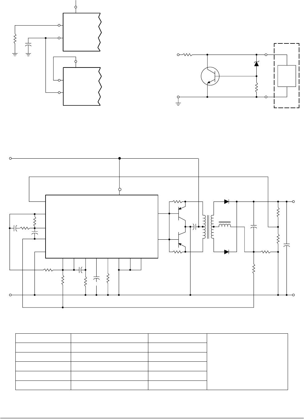
Figure 19. Slaving T
wo or More Control Circuits
Figure 20. Operation with V
in
> 40 V Using
External Zener
R
T
C
T
6
5
V
ref
R
T
C
T
Master
V
ref
Slave
(Additional
Circuits)
R
T
C
T
5
6
V
in
> 40V
R
S
V
Z
= 39V
1N975A
V
CC
5.0V
Ref
12
270
Gnd
7
+V
in
= 8.0V to 20V
1
2
3
15
16
+
−
−
+
Comp
OC
V
REF
DT
C
T
R
T
Gnd
E
1
E
2
1
3
1
4
45679
1
0
1.0M
33k
0.01
0.01
V
CC
C
1
C
2
8
11
47
47
10
+
10k
4.7k
4.7k
15k
Tip
32
+
T
1
1N4934
L
1
1N4934
240
+
50
35V
4.7k
1.0
22
k
+
+V
O
= 28V
I
O
= 0.2A
12
All capacitors in
m
F
TL594
0.001
50
35V
50
25V
Tip
32
Figure 21. Pulse Width Modulated Push−Pull Converter
T
est
Conditions
Results
L1 − 3.5 mH @ 0.3 A
T1 − Primary: 20T C.T
. #28 AWG
T1 −
Secondary: 12OT C.T
. #36
A
WG
T
1
−
Core: Ferroxcube
1408P−L00−3CB
Line Regulation
V
in
= 10 V to 40 V
14 mV 0.28%
Load Regulation
V
in
= 28 V
, I
O
= 1.0 mA to 1.0 A
3.0 mV 0.06%
Output Ripple
V
in
= 28 V
, I
O
= 1.0 A
65 mVpp P
.A.R.D.
Short Circuit Current
V
in
= 28 V
, R
L
= 0.1
W
1.6 A
Efficiency
V
in
= 28 V
, I
O
= 1.0 A
71%
P1-P3
P4-P6
P7-P9
P10-P12
TL594CDTBG
Mfr. #:
Buy TL594CDTBG
Manufacturer:
ON Semiconductor
Description:
Switching Controllers 40kHz 200mA PWM w/48% Duty Cycle Max
Lifecycle:
New from this manufacturer.
Delivery:
DHL
FedEx
Ups
TNT
EMS
Payment:
T/T
Paypal
Visa
MoneyGram
Western
Union
Products related to this Datasheet
TL594CDR2G
TL594CDTBR2G
TL594CN
TL594CDR2
TL594CDTBG
TL594CNG
TL594CDG