AH1893
Document number: DS35740 Rev. 1 - 2
1 of 10
www.diodes.com
July 2013
© Diodes Incorporated
NEW PRODUCT
A
H1893
HIGH SENSITIVITY MICROPOWER
OMNIPOLAR HALL-EFFECT SWITCH
Description
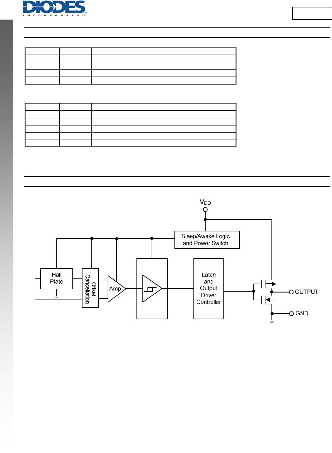
The AH1893 is a high sensitivity micropower Omnipolar Hall effect
switch IC with internal pull up and pull down capability. Designed for
portable and battery powered equipment such as cellular phones and
portable PCs to home appliances and industrial applications, the
average supply current is only 4.3µA at 1.85V. To support potable
equipment the AH1893 can operate over the supply range of 1.6V to
3.6V and uses a hibernating clocking system to minimize the power
consumption. To minimize PCB space the AH1893 is available in
small low profile X1-DFN1216-4 and SOT553 packages.
The output is activated with either a north or south pole of sufficient
magnetic field strength. When the magnetic flux density (B)
perpendicular to the package is larger than operate point (Bop), the
output will be turned on (pulled low) and held until B is lower than
release point (Brp).
Features
Omnipolar Operation (North or South pole)
Supply Voltage of 1.6V to 3.6V
High Sensitivity
Micropower Operation
Chopper Stabilized Design Provides
Superior Temperature Stability
Minimal Switch Point Drift
Enhanced Immunity to Physical Stress
No External Pull-up Resistors Required
Good RF Noise Immunity
-40°C to +85°C Operating Temperature
High ESD capability of 8kV (Human Body Model)
Small Low Profile SOT553 and X1-DFN1216-4 Packages
Totally Lead-Free & Fully RoHS Compliant (Notes 1 & 2)
Halogen and Antimony Free. “Green” Device (Note 3)
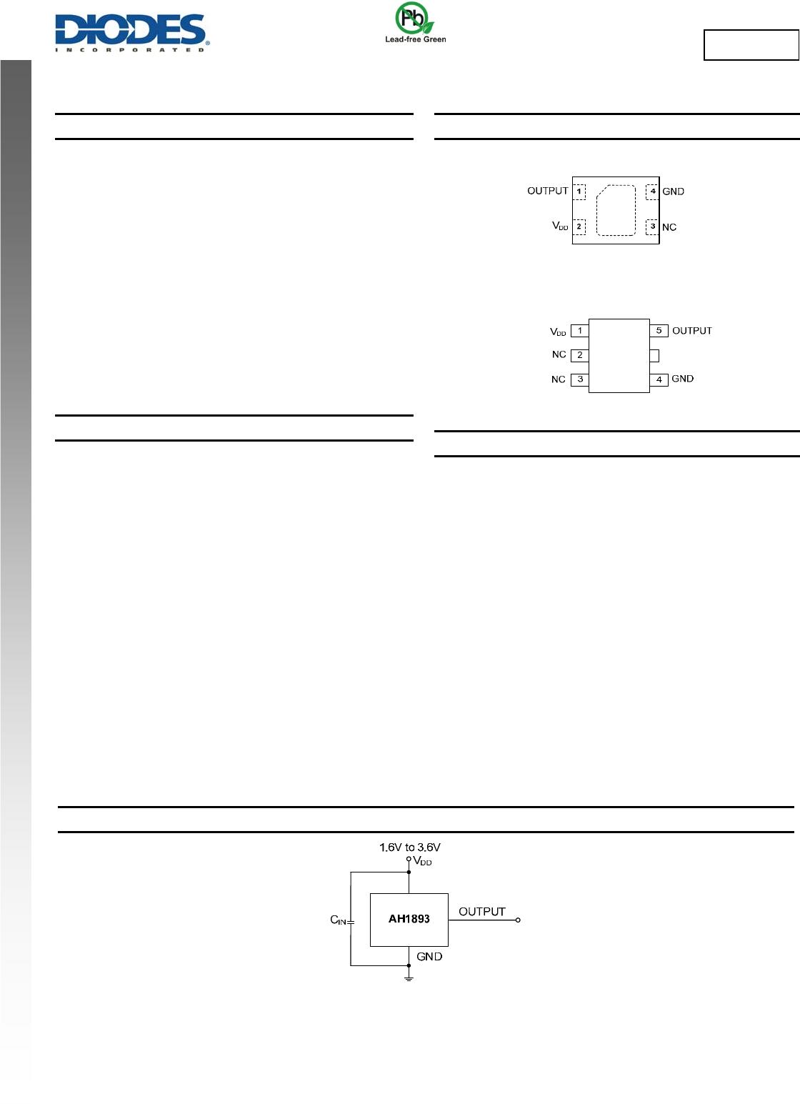
Pin Assignments
(Top View)
X1-DFN1216-4
(Top View)
SOT553
Applications
Open and Close Detect for Cellular Phones
Holster or Cover Detect for Cellular Phones and Tablet PCs
Cover or Display Switch in Portable PCs
Digital Still, Video Cameras and Handheld Gaming Consoles
Door, Lids and Tray Position Switches
Level, Proximity and Position Switches
Contact-Less Switches in Home Appliances and Industrial
Applications
Notes: 1. No purposely added lead. Fully EU Directive 2002/95/EC (RoHS) & 2011/65/EU (RoHS 2) compliant.
2. See http://www.diodes.com/quality/lead_free.html for more information about Diodes Incorporated’s definitions of Halogen- and Antimony-free, "Green"
and Lead-free.
3. Halogen- and Antimony-free "Green” products are defined as those which contain <900ppm bromine, <900ppm chlorine (<1500ppm total Br + Cl) and
<1000ppm antimony compounds.
Typical Applications Circuit
Note: 4. C
IN
is for power stabilization and to strengthen the noise immunity, the recommended capacitance is 100nF typical.
AH1893
Document number: DS35740 Rev. 1 - 2
2 of 10
www.diodes.com
July 2013
© Diodes Incorporated
NEW PRODUCT
A
H1893
Pin Descriptions
Package: X1-DFN1216-4
Pin Number Pin Name Function
1 OUTPUT Output Pin
2
V
DD
Power Supply Input
3 NC No Connection (Note 5)
4 GND Ground Pin
Package: SOT553
Pin Number Pin Name Function
1
V
DD
Power Supply Input
2 NC No Connection (Note 5)
3 NC No Connection (Note 5)
4 GND Ground
5 OUTPUT Output
Note: 5. NC is “No Connection” pin and is not connected internally. This pin can be left open or tied to ground.
Functional Block Diagram
AH1893
Document number: DS35740 Rev. 1 - 2
3 of 10
www.diodes.com
July 2013
© Diodes Incorporated
NEW PRODUCT
A
H1893
Absolute Maximum Ratings (Note 6) (@T
A
= +25°C, unless otherwise specified.)
Symbol Parameter Rating Unit
V
DD
Supply Voltage (Note 7) 6 V
V
DD_REV
Reverse Supply Voltage -0.3 V
I
OUTPUT
Output current (source and sink) 3 mA
B Magnetic Flux Density Unlimited
P
D
Package Power Dissipation
X1-DFN1216-4 230 mW
SOT553 230 mW
Ts Storage Temperature Range -65 to +150 °C
T
J
Maximum Junction Temperature 150 °C
ESD HBM Human Body Model (HMB) ESD capability 8 kV
Notes: 6. Stresses greater than the 'Absolute Maximum Ratings' specified above may cause permanent damage to the device. These are stress ratings only;
functional operation of the device at these or any other conditions exceeding those indicated in this specification is not implied. Device reliability may be
affected by exposure to absolute maximum rating conditions for extended periods of time.
7. The absolute maximum V
DD
of 6V is a transient stress rating and is not meant as a functional operating condition. It is not recommended to
operate the device at the absolute maximum rated conditions for any period of time.
Recommended Operating Conditions (@T
A
= +25°C, unless otherwise specified.)
Symbol Parameter Conditions Rating Unit
V
DD
Supply Voltage Operating 1.6V to 3.6V V
T
A
Operating Temperature Range Operating -40 to +85
C
Electrical Characteristics (@T
A
= +25°C, V
DD
= 1.85V, unless otherwise specified.)
Symbol Parameter Conditions Min Typ Max Unit
V
OL
Output Low Voltage (on) I
OUT
= 1mA - 0.1 0.2 V
V
OH
Output High Voltage (off) I
OUT
= -1mA V
DD
-0.2 V
DD
-0.1 — V
Ioff Output Leakage Current V
OUT
= 3.6V, Output IOff < 0.1 1 µA
I
DD
(awake)
Supply Current
During ‘Awake’ Period,
T
A
= +25°C, V
DD
= 3V
2.1 — mA
I
DD
(sleep)
During ‘Sleep’ Period,
T
A
= +25°C, V
DD
= 3V
2.5 — mA
I
DD
(avg)
Average Supply Current
T
A
= +25°C, V
DD
= 1.85V
4.3 8 µA
T
A
= +25°C, V
DD
= 3.6V
7.2 13 µA
Tawake Awake Time (Note 8) 50 100 µs
Tperiod Period (Note 8) 50 100 ms
D.C. Duty Cycle 0.1 — %
Note: 8. When power is initially turned on, the operating V
DD
(1.6V to 3.6V) must be applied to guaranteed the output sampling.
The output state is valid after the second operating cycle (typical 100ms).

AH1893-FA-7

Mfr. #:
Manufacturer:
Description:
Magnetic Sensors Board Mount Hall Effect / Magnetic Sensors Hall Effect Switch 1.6V to 3.6V 4.3uA
Lifecycle:
New from this manufacturer.
Delivery:
DHL FedEx Ups TNT EMS
Payment:
T/T Paypal Visa MoneyGram Western Union

Products related to this Datasheet