www.fairchildsemi.com 2
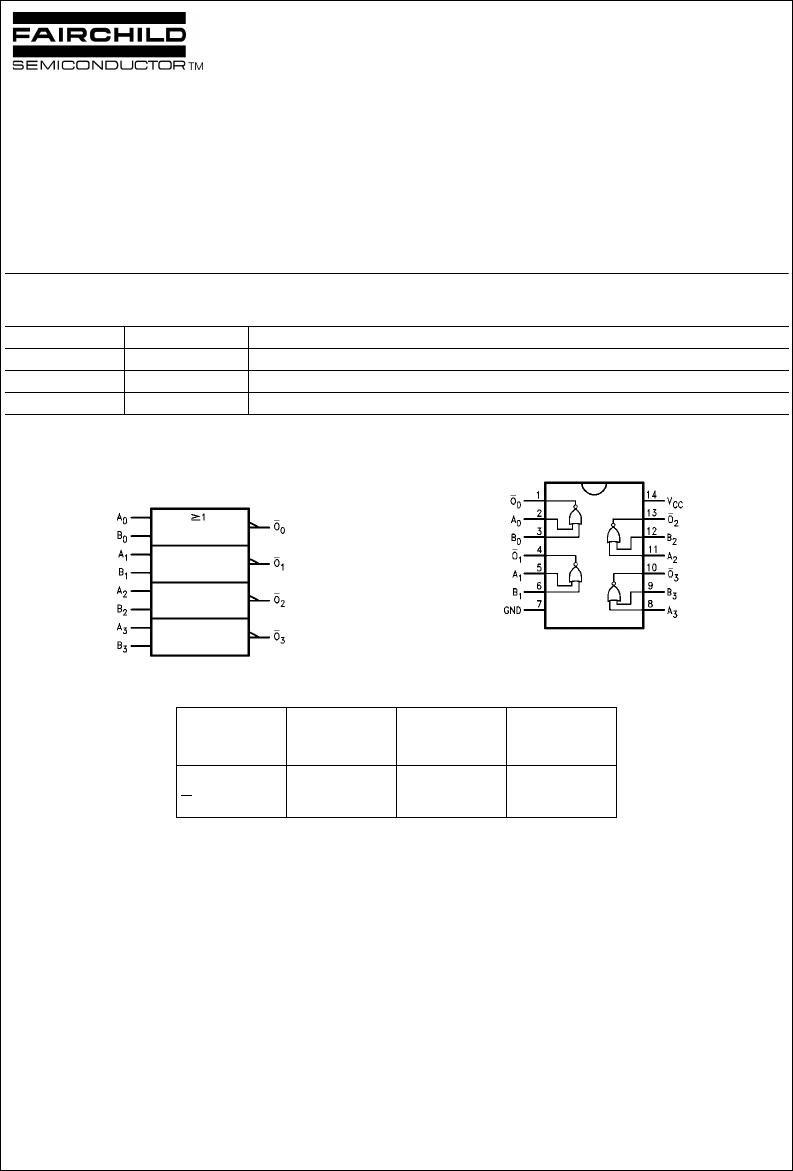
74F02
Absolute Maximum Ratings(Note 1) Recommended Operating
Conditions
Note 1: Absolute maximum ratings are values beyond which the device
may be damaged or have its useful life impaired. Functional operation
under these conditions is not implied.
Note 2: Either voltage limit or current limit is sufficient to protect inputs.
DC Electrical Characteristics
AC Electrical Characteristics
Storage Temperature −65°C to +150°C
Ambient Temperature under Bias
−55°C to +125°C
Junction Temperature under Bias
−55°C to +150°C
V
CC
Pin Potential to Ground Pin −0.5V to +7.0V
Input Voltage (Note 2)
−0.5V to +7.0V
Input Current (Note 2)
−30 mA to +5.0 mA
Voltage Applied to Output
in HIGH State (with V
CC
= 0V)
Standard Output
−0.5V to V
CC
3-STATE Output −0.5V to +5.5V
Current Applied to Output
in LOW State (Max) twice the rated I
OL
(mA)
Free Air Ambient Temperature 0
°C to +70°C
Supply Voltage
+4.5V to +5.5V
Symbol Parameter Min Typ Max Units
V
CC
Conditions
V
IH
Input HIGH Voltage 2.0 V Recognized as a HIGH Signal
V
IL
Input LOW Voltage 0.8 V Recognized as a LOW Signal
V
CD
Input Clamp Diode Voltage −1.2 V Min I
IN
= −18 mA
V
OH
Output HIGH 10% V
CC
2.5
VMin
I
OH
= −1 mA
Voltage 5% V
CC
2.7 I
OH
= −1 mA
V
OL
Output LOW 10% V
CC
0.5 V Min I
OL
= 20 mA
Voltage
I
IH
Input HIGH
5.0 µAMaxV
IN
= 2.7V
Current
I
BVI
Input HIGH Current
7.0 µAMaxV
IN
= 7.0V
Breakdown Test
I
CEX
Output HIGH
50 µAMaxV
OUT
= V
CC
Leakage Current
V
ID
Input Leakage
4.75 V 0.0
I
ID
= 1.9 µA
Test All other pins grounded
I
OD
Output Leakage
3.75 µA0.0
V
IOD
= 150 mV
Circuit Current All other pins grounded
I
IL
Input LOW Current −0.6 mA Max V
IN
= 0.5V
I
OS
Output Short-Circuit Current −60 −150 mA Max V
OUT
= 0V
I
CCH
Power Supply Current 3.7 5.6 mA Max V
O
= HIGH
I
CCL
Power Supply Current 8.7 13.0 mA Max V
O
= LOW
Symbol Parameter
T
A
= +25°CT
A
= −55°C to +125°CT
A
= 0°C to +70°C
Units
V
CC
= +5.0V V
CC
= +5.0V V
CC
= +5.0V
C
L
= 50 pF C
L
= 50 pF C
L
= 50 pF
Min Typ Max Min Max Min Max
t
PLH
Propagation Delay 2.5 4.4 5.5 2.5 7.5 2.5 6.5
ns
t
PHL
A
n
, B
n
to O
n
1.5 3.2 4.3 1.5 6.5 1.5 5.3