–6–
AD1854
REV. A
OPERATING FEATURES
Serial Data Input Port
The AD1854’s flexible serial data input port accepts data in
twos-complement, MSB-first format. The left channel data field
always precedes the right channel data field. The input data
consists of either 16, 18, 20, or 24 bits, as established by the
mode select pins (IDPM0 Pin 21 and IDPM1 Pin 20) or the
mode select bits (Bits 15 and 14) in the control register through
the SPI (Serial Peripheral Interface) control port. Neither the
pins nor the SPI controls has preference; to ensure proper control,
the selection not being used should be tied LO. Therefore,
when the SPI bits are used to control Serial Data Input Format,
Pins 20 and 21 should be tied LO. Similarly, when the pins are
to be used to select the Data Format, the SPI bits should be set
to zeros. When the SPI Control Port is not being used, the SPI
Pins (3, 4, and 5) should be tied LO.
Serial Data Input Mode
The AD1854 uses two multiplexed input pins to control the
mode configuration of the input data port mode as follows:
Table I. Serial Data Input Modes
IDPM1 IDPM0
(Pin 20) (Pin 21) Serial Data Input Format
0 0 Right Justified (16 Bits)
01 I
2
S-Compatible
1 0 Right Justified (20 Bits)
1 1 Right Justified (24 Bits)
Bit Clock 0 Left Justified
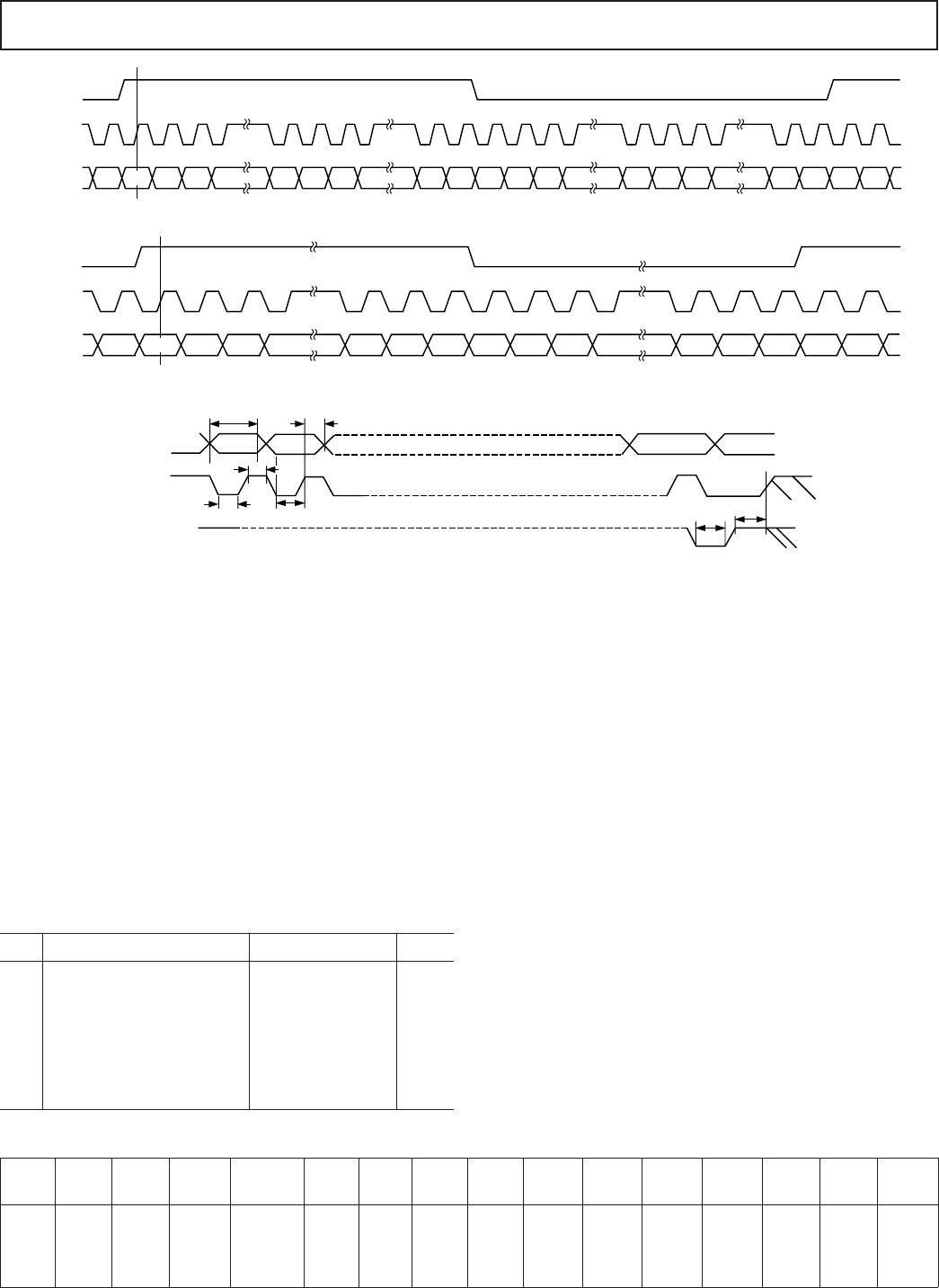
Figure 1 shows the right-justified mode (16-bit mode). L/RCLK
is HI for the left channel, LO for the right channel. Data is valid
on the rising edge of BCLK. The MSB is delayed 16-bit clock
periods from an L/RCLK transition, so that when there are 64
BCLK periods per L/RCLK period, the LSB of the data will be
right justified to the next L/RCLK transition. The right-justified
mode can also be used with 20-bit or 24-bit inputs as selected
in Table I.
Figure 2 shows the I
2
S-justified mode. L/RCLK is LO for the
left channel and HI for the right channel. Data is valid on the
rising edge of BCLK. The MSB is left justified to an L/RCLK
transition but with a single BCLK period delay. The I
2
S-justified
mode can be used with 16-/18-/20- or 24-bit inputs.
Figure 3 shows the left-justified mode. Note: Left-justified mode
is selected by pulsing IDPM1 (Pin 20) with bit clock, that is, tying
bit clock to IDPM1 while IDPM0 (Pin 21) is tied LO. Left-
justified can only be selected this way, it cannot be selected through
SPI Control Port.
L/RCLK is HI for the left channel, and LO for the right channel.
Data is valid on the rising edge of BCLK. The MSB is left-
justified to an L/RCLK transition, with no MSB delay. The
left-justified mode can be used with 16-/18-/20- or 24-bit inputs.
Note that the AD1854 is capable of a 32 × F
S
BCLK frequency
“packed mode” where the MSB is left-justified to an L/RCLK
transition, and the LSB is right-justified to an L/RCLK transi-
tion. L/RCLK is HI for the left channel, and LO for the right
channel. Data is valid on the rising edge of BCLK. Packed
mode can be used when the AD1854 is programmed in right-
justified mode. Packed mode is shown is Figure 4.
Table II. Frequency Mode Settings
F
S
96/48 MCLK X2MCLK 384/256 Note
Normal, 32 kHz–48 kHz 0 256 × F
S
00
Normal, 32 kHz–48 kHz 0 384 × F
S
01
Normal, 32 kHz–48 kHz 0 512 × F
S
10
Normal, 32 kHz–48 kHz 0 1 1 Not Allowed
Double F
S
(96 kHz) 1 128 × F
S
00
Double F
S
(96 kHz) 1 (384/2) × F
S
01
Double F
S
(96 kHz) 1 256 × F
S
10
Double F
S
(96 kHz) 1 1 1 Not Allowed
SDATA
INPUT
LSBMSB2MSB1 LSB+2 LSB+1
MSB 2
MSB 1
MSB
LSB+2
LSB+1
LSB
BCLK
INPUT
L/RCLK
INPUT
LEFT CHANNEL
RIGHT CHANNEL
MSB
LSB
Figure 1. Right-Justified Mode
LEFT CHANNEL
RIGHT CHANNEL
MSB2MSB1 LSB+2 LSB+1 LSB MSB2MSB1MSB LSB+2 LSB+1 LSB MSB
L/RCLK
INPUT
BCLK
INPUT
SDATA
INPUT
MSB
Figure 2. I
2
S-Justified Mode
AD1854
7REV. A
MSB2MSB1 LSB+2 LSB+1 LSB MSB2MSB1MSB LSB+2 LSB+1 LSB MSB1MSB
L/RCLK
INPUT
BCLK
INPUT
SDATA
INPUT
LEFT CHANNEL
RIGHT CHANNEL
MSB
Figure 3. Left-Justified Mode
L/RCLK
INPUT
LEFT CHANNEL
RIGHT CHANNEL
BCLK
INPUT
SDATA
INPUT
LSB MSB1 MSB2 LSB+2 LSB+1 LSB MSB MSB1 MSB2 LSB+2 LSB+1 LSB MSB MSB1MSB
Figure 4. 32
×
F
S
Packed Mode
D15
D14
D0
t
CHD
t
CCH
t
CSU
t
CCL
t
CLL
t
CLH
CDATA
CCLK
CLATCH
t
CCP
Figure 5. Serial Control Port Timing
Serial Control Port
The AD1854 serial control port is SPI-compatible. SPI (Serial
Peripheral Interface) is an industry standard serial port protocol.
The write-only serial control port gives the user access to: select
input mode, soft power-down control, soft de-emphasis, channel-
specific attenuation and mute (both channels at once). The
AD1854 serial control port consists of three signals, control
clock CCLK (Pin 4), control data CDATA (Pin 5), and control
latch CLATCH (Pin 3). The control data input must be valid
on the control clock rising edge, and the control clock must make a
LO to HI transition when there is valid data. The control latch
must make a LO-to-HI transition after the LSB has been clocked
into the AD1854, while the control clock is inactive. The timing
relation between these signals is shown in Figure 5. The control
bits are assigned as in Table IV.
Table III. Digital Timing
Min Unit
t
CCH
CCLK HI Pulsewidth 40 (Burst Mode) ns
t
CCL
CCLK LO Pulsewidth 40 (Burst Mode) ns
t
CCP
CCLK Period 80 (Burst Mode) ns
t
CSU
CDATA Setup Time 10 ns
t
CHD
CDATA Hold Time 10 ns
t
CLL
CLATCH LO Pulsewidth 10 ns
t
CLH
CLATCH HI Pulsewidth 130 (Burst Mode) ns
The serial control port is byte oriented. The data is MSB first,
and is unsigned. There is one control register for the left
channel or the right channel, as distinguished by Bit Data 10.
For power-up and reset, the default settings are: Data 11 the
mute control bit, reset default state is LO, which is the normal
(nonmuted) setting. Data 10 is LO, the Volume 9 through
Volume 0 control bits have a reset default value of 11 1111 1111,
which is an attenuation of 0.0 dB (i.e., full scale, no attenuation).
The intent with these reset defaults is to enable AD1854 applica-
tions without requiring the use of the serial control port. For those
users who do not use the serial control port, it is still possible to
mute the AD1854 output by using the MUTE (Pin 23) signal.
Note that the serial control port timing is asynchronous to the
serial data port timing. Changes made to the attenuator level
will be updated on the next edge of the L/RCLK after the
CLATCH write pulse as shown in Figure 8.
The SPI port can be used in either of two modes, Burst Mode,
or Continuous CCLK Mode, as described below.
Continuous CCLK Mode
In this mode, the maximum CCLK frequency is 3 MHz. The
CCLK can run continuously between transactions. Please note
that the LO-to-HI transition of the CLATCH with respect to
the rising edge of CCLK must be at least 130 ns, as shown in
Figure 6.
Table IV. Serial Control Bit Definitions
MSB LSB
Data 15 Data 14 Data 13 Data 12 Data 11 Data 10 Data 9 Data 8 Data 7 Data 6 Data 5 Data 4 Data 3 Data 2 Data 1 Data 0
IDPM1 IDPM0 Soft Soft 1/Mute 1/Right Volume Volume Volume Volume Volume Volume Volume Volume Volume Volume
Input Input Power- De- 0/Normal 0/Left Control Control Control Control Control Control Control Control Control Control
Mode1 Mode0 Down Emphasis (Nonmute) Data Data Data Data Data Data Data Data Data Data
Select Select
8
AD1854
REV. A
Burst Mode
To operate with SPI CCLK frequencies up to 12.288 MHz, the
SPI port can be operated in Burst Mode. This means that when
CLATCH is high, CCLK cannot be HI, as shown in Figure 7.
Mute
The AD1854 offers two methods of muting the analog output.
By asserting the MUTE (Pin 23) signal HI, both the left and
right channel are muted. As an alternative, the user can assert
the mute bit in the serial control register (Data 11) HI. The
AD1854 has been designed to minimize pops and clicks when
muting and unmuting the device.
Smooth Volume Control with Auto Ramp Up/Down
The AD1854 incorporates ADI’s 1024 step “Smooth Volume
Control” with auto ramp up/down. Once per L/RCLK cycle, the
AD1854 compares current volume level register to the volume
level request register Data 9:0. If different, volume is adjusted
one step/sample. Therefore, a change from max to min volume
takes 1024 samples or about 20 ms as shown in Figure 8.
20ms
TIME
60
60
0
0
LEVEL dB
VOLUME REQUEST REGISTER
ACTUAL VOLUME REGISTER
Figure 8. Smooth Volume Control
Output Drive, Buffering and Loading
The AD1854 analog output stage is able to drive a 1 k (in
series with 2 nF) load.
Power-Down Reset
The AD1854 offers two methods for power-down and reset.
When the PD/RST input (Pin 24) is asserted LO, the AD1854
is reset. As an alternative, the user can assert the soft power-
down bit (Data 13) HI. All the registers in the AD1854 digital
engine (serial data port, interpolation filter and modulator) are
zeroed. The two 8-bit registers in the serial control port are
initialized back to their default values. The user should wait
100 ms after bringing PD/RST HI before using the serial data
input port and the serial control input. The AD1854 is designed
to minimize pops and clicks when entering and exiting the power-
down state.
De-Emphasis
The AD1854 offers digital de-emphasis, supporting 50 µs/15 µs
digital de-emphasis intended for “Redbook” 44.1 kHz sample
frequency playback from Compact Discs. The AD1854 offers
control of de-emphasis by asserting the DEEMP input (Pin 9)
HI or by asserting the de-emphasis register bit (Data 12) HI.
The AD1854’s de-emphasis is optimized for 44.1 kHz but will
scale to the other sample frequencies.
Control Signals
The IDPM0, IDPM1, and DEEMP control inputs are normally
connected HI or LO to establish the operating state of the
AD1854. They can be changed dynamically (and asynchronously
to L/RCLK and the master clock) as long as they are stable
before the first serial data input bit (i.e., MSB) is presented to
the AD1854.
CLATCH
CCLK
20 40 60 80 100 120 140 160 180
CDATA
>130ns
TIME ns
Figure 6. SPI Port Continuous CCLK Mode
CLATCH
CCLK
CDATA
TIME ns
200 400 600 800 1000 1200 1400 1600 1800
Figure 7. SPI Port Burst Mode

AD1854JRSZRL

Mfr. #:
Manufacturer:
Analog Devices Inc.
Description:
Audio D/A Converter ICs Stereo 96KHz Multibt IC
Lifecycle:
New from this manufacturer.
Delivery:
DHL FedEx Ups TNT EMS
Payment:
T/T Paypal Visa MoneyGram Western Union

Products related to this Datasheet