10
LTC1864L/LTC1865L
sn18645L 18645Lfs
LTC1865L OPERATION
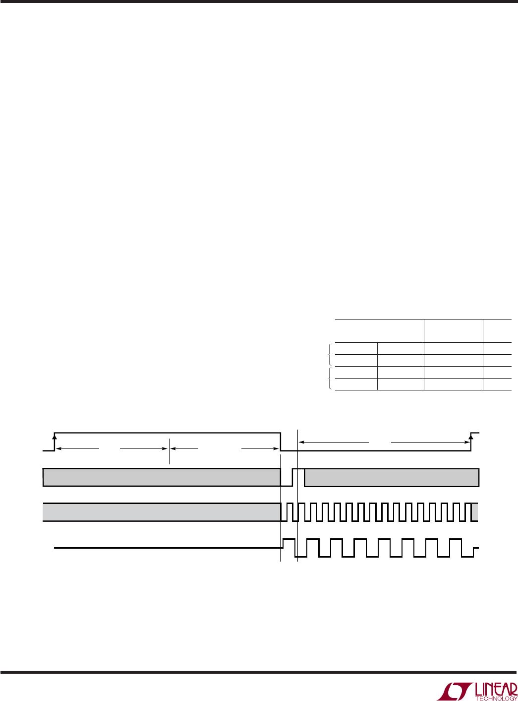
Operating Sequence
The LTC1865L conversion cycle begins with the rising
edge of CONV. After a period equal to t
CONV
, the conver-
sion is finished. If CONV is left high after this time, the
LTC1865L goes into sleep mode drawing only leakage
current. The LTC1865L’s 2-bit data word is clocked into
the SDI input on the rising edge of SCK after CONV goes
low. Additional inputs on the SDI pin are then ignored until
the next CONV cycle. The shift clock (SCK) synchronizes
the data transfer with each bit being transmitted on the
falling SCK edge and captured on the rising SCK edge in
both transmitting and receiving systems. The data is
transmitted and received simultaneously (full duplex).
After completing the data transfer, if further SCK clocks
are applied with CONV low, SDO will output zeros indefi-
nitely. See Figure 4.
Analog Inputs
The two bits of the input word (SDI) assign the MUX
configuration for the next requested conversion. For a
given channel selection, the converter will measure the
voltage between the two channels indicated by the
“+” and “–” signs in the selected row of Table 1. In
CONV
SDI
SCK
16151413121110987654321
SDO
B15
B14 B12 B10 B8 B6 B4 B2
B0*
Hi-Z
B13
B11 B9 B7 B5 B3 B1
S/D O/S
DON’T CAREDON’T CARE
t
CONV
1864 F04
SLEEP MODE
*AFTER COMPLETING THE DATA TRANSFER, IF FURTHER SCK CLOCKS ARE
APPLIED WITH CONV LOW, THE ADC WILL OUTPUT ZEROS INDEFINITELY
Hi-Z
t
SMPL
DON'T CARE
Figure 4. LTC1865L Operating Sequence
APPLICATIO S I FOR ATIO
WUUU
MUX ADDRESS
Table 1. Multiplexer Channel Selection
SGL/DIFF
1
1
0
0
ODD/SIGN
0
1
0
1
CHANNEL #
0
+
+
–
1
+
–
+
GND
–
–
1864 TBL1
SINGLE-ENDED
MUX MODE
DIFFERENTIAL
MUX MODE
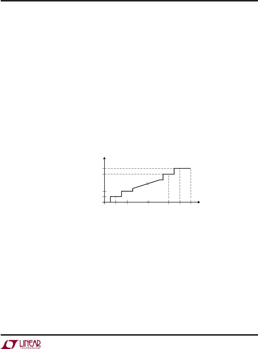
single-ended mode, all input channels are measured with
respect to GND. A zero code will occur when the “+” input
minus the “–” input equals zero. Full scale occurs when
the “+” input minus the “–” input equals V
REF
minus
1LSB. See Figure 5. Both the “+” and “–” inputs are
sampled at the same time so common mode noise is
rejected. The input span in the SO-8 package is fixed at
V
REF
= V
CC
. If the “–” input in differential mode is
grounded, a rail-to-rail input span will result on the “+”
input.
Reference Input
The reference input of the LTC1865L SO-8 package is
internally tied to V
CC
. The span of the A/D converter is
therefore equal to V
CC
. The voltage on the reference input
of the LTC1865L MSOP package defines the span of the
A/D converter. The LTC1865L MSOP package can operate
with reference voltages from 1V to V
CC
.