Nexperia
74AVC4T774
4-bit dual supply translating transceiver; 3-state
74AVC4T774 All information provided in this document is subject to legal disclaimers. © Nexperia B.V. 2017. All rights reserved.
Product data sheet Rev. 1 — 25 September 2017
10 / 26
11 Dynamic characteristics
Table 10. Typical power dissipation capacitance at V
CC(A)
= V
CC(B)
and T
amb
= 25 °C
[1]
[2]
Voltages are referenced to GND (ground = 0 V).
V
CC(A)
= V
CC(B)
Symbol Parameter Conditions
0.8 V 1.2 V 1.5 V 1.8 V 2.5 V 3.3 V
Unit
A port: (direction An to Bn);
output enabled
0.2 0.2 0.2 0.2 0.3 0.4 pF
A port: (direction An to Bn);
output disabled
0.2 0.2 0.2 0.2 0.3 0.4 pF
A port: (direction Bn to An);
output enabled
9.5 9.7 9.8 9.9 10.7 11.9 pF
A port: (direction Bn to An);
output disabled
0.6 0.6 0.6 0.6 0.7 0.7 pF
B port: (direction An to Bn);
output enabled
9.5 9.7 9.8 9.9 10.7 11.9 pF
B port: (direction An to Bn);
output disabled
0.6 0.6 0.6 0.6 0.7 0.7 pF
B port: (direction Bn to An);
output enabled
0.2 0.2 0.2 0.2 0.3 0.4 pF
C
PD
power dissipation
capacitance
B port: (direction Bn to An);
output disabled
0.2 0.2 0.2 0.2 0.3 0.4 pF
[1] C
PD
is used to determine the dynamic power dissipation (P
D
in μW).
P
D
= C
PD
x V
CC
2
× f
i
x N + Σ(C
L
x V
CC
2
× f
o
) where:
f
i
= input frequency in MHz;
f
o
= output frequency in MHz;
C
L
= load capacitance in pF;
V
CC
= supply voltage in V;
N = number of inputs switching;
Σ(C
L
x V
CC
2
x f
o
) = sum of the outputs.
[2] f
i
= 10 MHz; V
I
= GND to V
CC
; t
r
= t
f
= 1 ns; C
L
= 0 pF; R
L
= ∞ Ω.
Nexperia
74AVC4T774
4-bit dual supply translating transceiver; 3-state
74AVC4T774 All information provided in this document is subject to legal disclaimers. © Nexperia B.V. 2017. All rights reserved.
Product data sheet Rev. 1 — 25 September 2017
11 / 26
Table 11. Typical dynamic characteristics at V
CC(A)
= 0.8 V and T
amb
= 25 °C
[1]
Voltages are referenced to GND (ground = 0 V); for test circuit see Figure 7; for waveforms see Figure 5 and Figure 6
V
CC(B)
Symbol Parameter Conditions
0.8 V 1.2 V 1.5 V 1.8 V 2.5 V 3.3 V
Unit
An to Bn 14.5 7.3 6.5 6.2 5.9 6.0 nst
pd
propagation delay
Bn to An 14.5 12.7 12.4 12.3 12.1 12.0 ns
OE to An 14.3 14.3 14.3 14.3 14.3 14.3 nst
dis
disable time
OE to Bn 17.0 9.9 9.0 9.4 9.0 9.7 ns
OE to An 18.2 18.2 18.2 18.2 18.2 18.2 nst
en
enable time
OE to Bn 19.2 10.7 9.8 9.6 9.7 10.2 ns
[1] t
pd
is the same as t
PLH
and t
PHL
; t
dis
is the same as t
PLZ
and t
PHZ
; t
en
is the same as t
PZL
and t
PZH
.
Table 12. Typical dynamic characteristics at V
CC(B)
= 0.8 V and T
amb
= 25 °C
[1]
Voltages are referenced to GND (ground = 0 V); for test circuit see Figure 7; for waveforms see Figure 5 and Figure 6
V
CC(A)
Symbol Parameter Conditions
0.8 V 1.2 V 1.5 V 1.8 V 2.5 V 3.3 V
Unit
An to Bn 14.5 12.7 12.4 12.3 12.1 12.0 nst
pd
propagation delay
Bn to An 14.5 7.3 6.5 6.2 5.9 6.0 ns
OE to An 14.3 5.5 4.1 4.0 3.0 3.5 nst
dis
disable time
OE to Bn 17.0 13.8 13.4 13.1 12.9 12.7 ns
OE to An 18.2 5.6 4.0 3.2 2.4 2.2 nst
en
enable time
OE to Bn 19.2 14.6 14.1 13.9 13.7 13.6 ns
[1] t
pd
is the same as t
PLH
and t
PHL
; t
dis
is the same as t
PLZ
and t
PHZ
; t
en
is the same as t
PZL
and t
PZH
.
Nexperia
74AVC4T774
4-bit dual supply translating transceiver; 3-state
74AVC4T774 All information provided in this document is subject to legal disclaimers. © Nexperia B.V. 2017. All rights reserved.
Product data sheet Rev. 1 — 25 September 2017
12 / 26
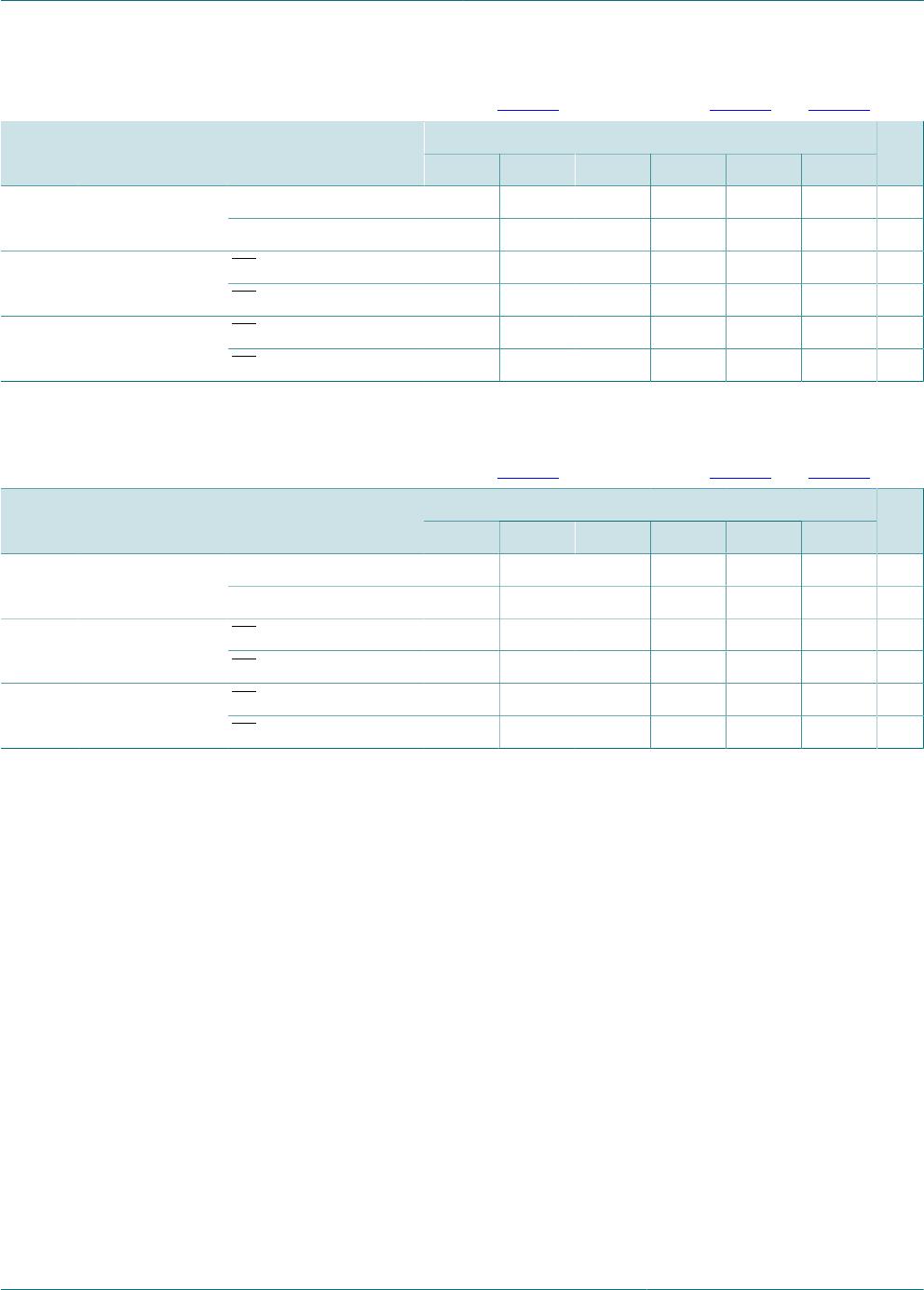
Table 13. Dynamic characteristics for temperature range -40 °C to +85 °C
[1]
Voltages are referenced to GND (ground = 0 V); for test circuit see Figure 7; for waveforms see Figure 5 and Figure 6
V
CC(B)
1.2 V ±0.1 V 1.5 V ±0.1 V 1.8 V ±0.15 V 2.5 V ±0.2 V 3.3 V ±0.3 V
Symbol Parameter Conditions
Min Max Min Max Min Max Min Max Min Max
Unit
V
CC(A)
= 1.1 V to 1.3 V
An to Bn 2.0 10.5 1.3 7.8 1.2 6.9 1.0 5.9 0.8 5.7 nst
pd
propagation
delay
Bn to An 2.0 10.5 1.5 9.9 1.5 9.7 1.4 9.4 1.4 9.3 ns
OE to An 2.0 10.0 2.0 10.0 2.0 10.0 2.0 10.0 2.0 10.0 nst
dis
disable time
OE to Bn 2.0 11.1 2.0 8.6 1.0 8.0 0.7 7.0 1.0 8.0 ns
OE to An 2.0 13.5 2.0 13.5 2.0 13.5 2.0 13.5 2.0 13.5 nst
en
enable time
OE to Bn 2.0 15.0 2.0 11.0 2.0 9.4 1.0 7.8 1.0 7.4 ns
V
CC(A)
= 1.4 V to 1.6 V
An to Bn 1.5 9.9 1.0 7.1 1.0 6.0 0.5 4.8 0.5 4.3 nst
pd
propagation
delay
Bn to An 1.3 7.8 1.0 7.1 0.9 6.9 0.8 6.6 0.6 6.5 ns
OE to An 1.0 6.0 1.0 6.0 1.0 6.0 1.0 6.0 1.0 6.0 nst
dis
disable time
OE to Bn 2.0 10.2 1.5 7.5 0.9 7.2 0.4 6.2 0.4 6.1 ns
OE to An 1.0 7.5 1.0 7.5 1.0 7.5 1.0 7.5 1.0 7.5 nst
en
enable time
OE to Bn 2.0 14.4 1.4 7.9 1.3 7.7 1.1 6.4 1.1 5.6 ns
V
CC(A)
= 1.65 V to 1.95 V
An to Bn 1.5 9.7 0.9 6.9 0.8 5.7 0.5 4.5 0.3 4.0 nst
pd
propagation
delay
Bn to An 1.2 6.9 1.0 6.0 0.8 5.7 0.5 5.5 0.5 5.3 ns
OE to An 0.5 5.7 0.5 5.7 0.5 5.7 0.5 5.7 0.5 5.7 nst
dis
disable time
OE to Bn 2.0 9.9 1.5 7.0 0.8 6.9 0.2 5.8 0.2 5.9 ns
OE to An 1.0 6.7 1.0 6.7 1.0 6.7 1.0 6.7 1.0 6.7 nst
en
enable time
OE to Bn 1.5 13.9 1.2 7.2 1.2 6.9 0.8 5.4 0.6 5.0 ns
V
CC(A)
= 2.3 V to 2.7 V
An to Bn 1.4 9.4 0.8 6.6 0.5 5.5 0.4 4.2 0.2 3.7 nst
pd
propagation
delay
Bn to An 1.0 5.9 0.5 4.8 0.5 4.5 0.4 4.2 0.3 3.9 ns
OE to An 0.2 4.0 0.2 4.0 0.2 4.0 0.2 4.0 0.2 4.0 nst
dis
disable time
OE to Bn 2.0 9.3 1.5 6.7 0.7 6.3 0.2 5.0 0.2 5.7 ns
OE to An 0.6 4.5 0.6 4.5 0.6 4.5 0.6 4.5 0.6 4.5 nst
en
enable time
OE to Bn 1.5 13.6 1.0 6.8 1.0 6.0 0.8 4.6 0.6 4.2 ns

74AVC4T774BQX

Mfr. #:
Manufacturer:
Nexperia
Description:
Translation - Voltage Levels 74AVC4T774BQ/SOT763/DHVQFN16
Lifecycle:
New from this manufacturer.
Delivery:
DHL FedEx Ups TNT EMS
Payment:
T/T Paypal Visa MoneyGram Western Union

Products related to this Datasheet